Transistor with an oxide semiconductor layer
a semiconductor layer and semiconductor technology, applied in the direction of semiconductors, semiconductor devices, electrical equipment, etc., can solve the problems of insufficient electric field applied to the semiconductor layer from the gate electrode layer formed adjacent to the side surface of the semiconductor layer, and the horizontal transistor cannot be said to be suitable for a semiconductor device for high power applications, etc., to achieve high drain-breakdown voltage characteristics, good properties, and high power applications
- Summary
- Abstract
- Description
- Claims
- Application Information
AI Technical Summary
Benefits of technology
Problems solved by technology
Method used
Image

Examples
embodiment 1
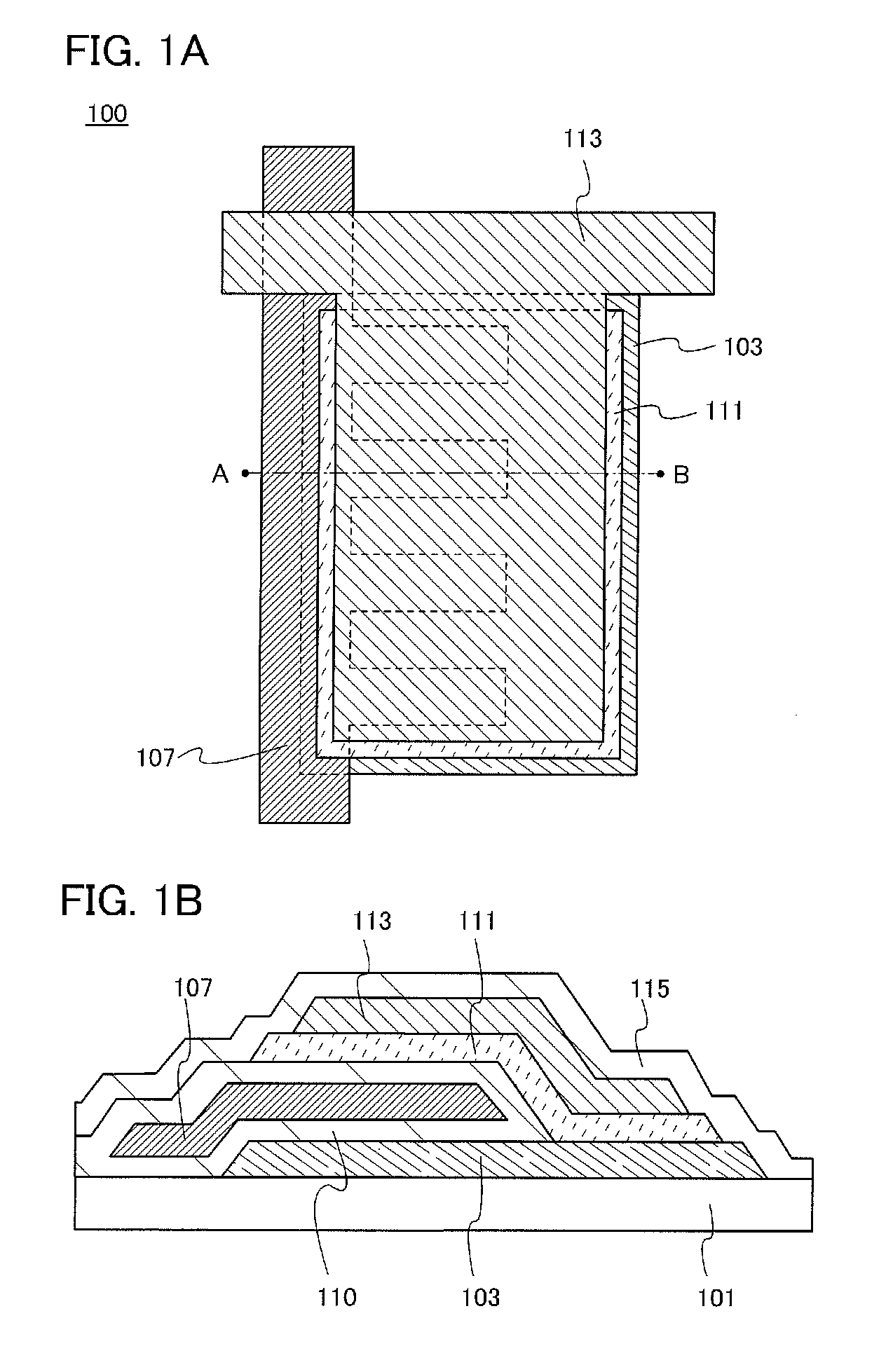
[0038]In this embodiment, a structure of a transistor 100 will be described with reference to FIGS. 1A and 1B.
[0039]FIG. 1A is a top view of the transistor 100, and FIG. 1B corresponds to a cross-sectional view taken along dashed line A-B in FIG. 1A.
[0040]As illustrated in FIG. 1B, a source electrode layer 103 is provided over a substrate 101, and a gate insulating layer 110 and a gate electrode layer 107 are provided over the source electrode layer 103. The gate insulating layer 110 covers an upper surface and a bottom surface of the gate electrode layer 107 and is in contact with the source electrode layer 103. Further, a bottom surface of an oxide semiconductor layer 111 is in contact with part of the gate insulating layer 110 and part of the source electrode layer 103. In addition, a drain electrode layer 113 is provided over the oxide semiconductor layer 111, and a protective insulating layer 115 is provided over the outermost layer of the transistor 100.
[0041]In the transistor...
embodiment 2
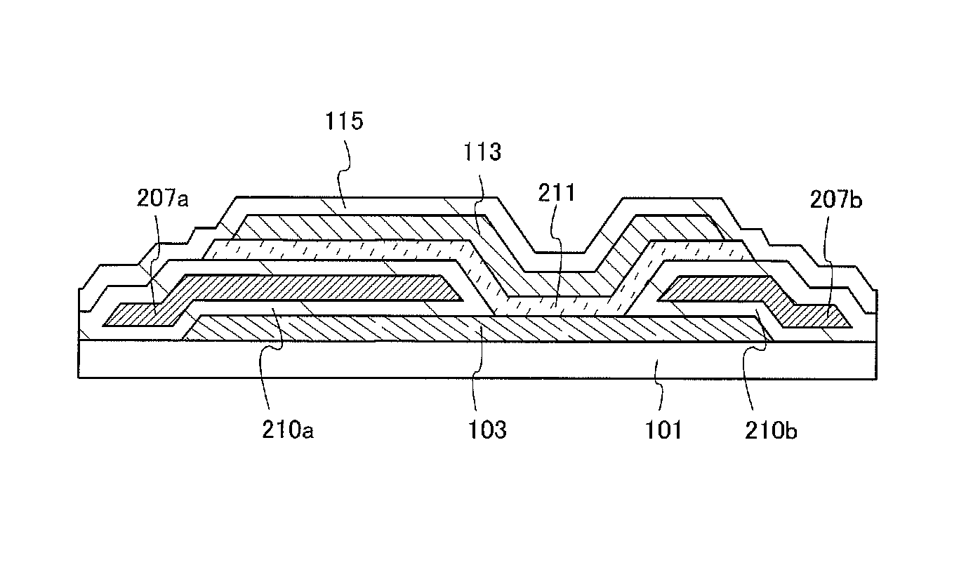
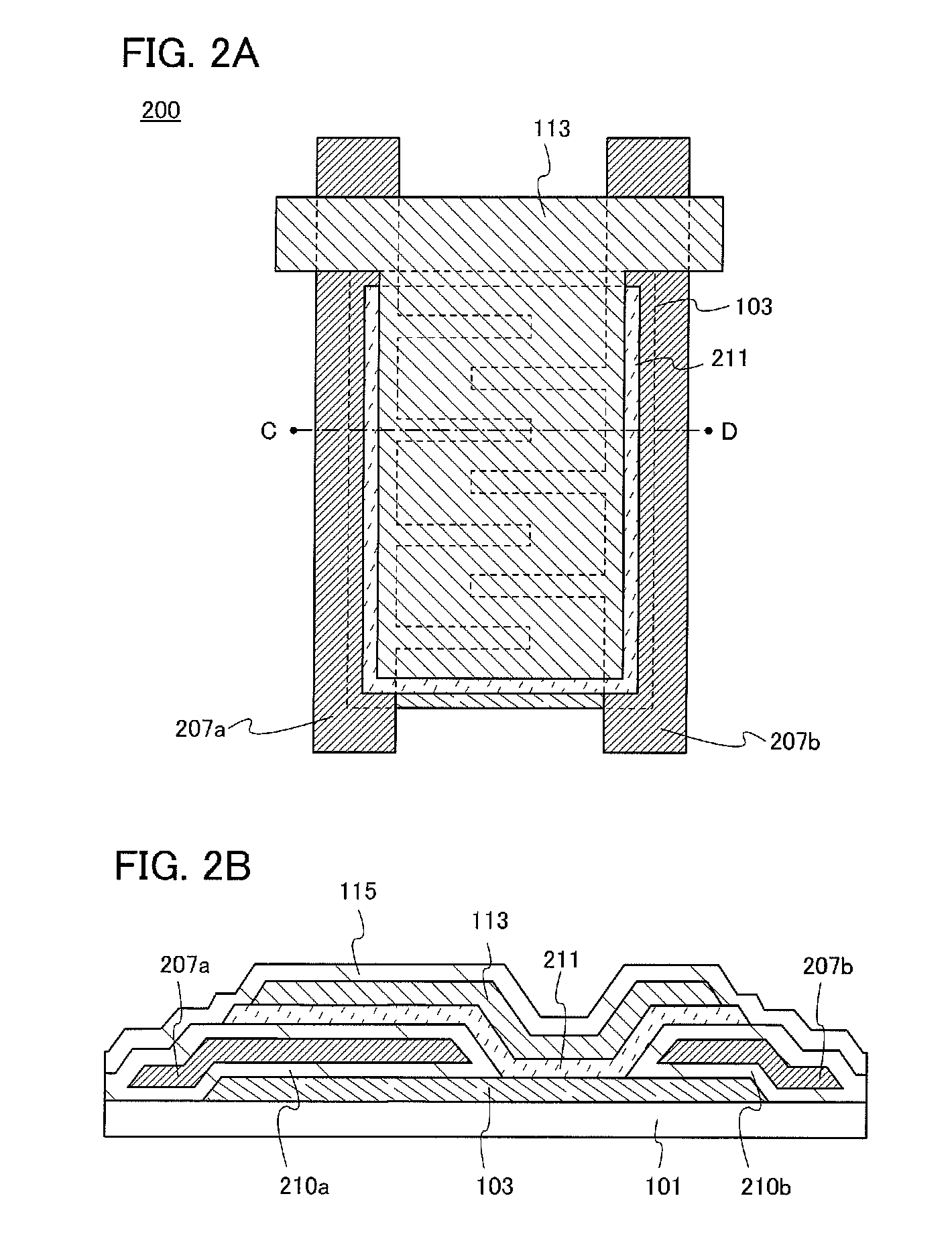
[0068]In this embodiment, a transistor 200 having a structure which is partly different from the structure of the transistor 100 described in Embodiment 1 will be described with reference to FIGS. 2A and 2B.
[0069]FIG. 2A is a top view of the transistor 200, and FIG. 2B corresponds to a cross-sectional view taken along dashed line C-D in FIG. 2A.
[0070]As illustrated in FIG. 2B, the source electrode layer 103 is provided over the substrate 101, and gate insulating layers 210a and 210b and gate electrode layers 207a and 207b are provided over the source electrode layer 103. The gate insulating layers 210a and 210b cover upper surfaces and bottom surfaces of the gate electrode layers 207a and 207b and are in contact with the source electrode layer 103. In addition, an oxide semiconductor layer 211 is provided so as to cover parts of the gate insulating layers 210a and 210b and to be in contact with part of the electrode layer 103. Further, the drain electrode layer 113 is provided on an...
embodiment 3
[0079]In this embodiment, a transistor 300 having a structure which is partly different from the structure of the transistor 200 described in Embodiment 2 will be described with reference to FIGS. 3A and 3B.
[0080]FIG. 3A is a top view of the transistor 300, and FIG. 3B corresponds to a cross-sectional view taken along dashed line E-F in FIG. 3A.
[0081]As illustrated in FIG. 3B, the source electrode layer 103 is provided over the substrate 101, and an oxide semiconductor layer 311, gate insulating layers 310a and 310b, and gate electrode layers 307a and 307b are provided over the source electrode layer 103. The gate insulating layers 310a and 310b cover upper surfaces and bottom surfaces of the gate electrode layers 307a and 307b. The oxide semiconductor layer 311 is in contact with the source electrode layer 103. Portions of the gate insulating layers 310a and 3106 and the gate electrode layers 307a and 307b which overlap with the source electrode layer 103 are covered with the oxide...
PUM
 Abstract
Description
Claims
Application Information
 - R&D
- Intellectual Property
- Life Sciences
- Materials
- Tech Scout
- Unparalleled Data Quality
- Higher Quality Content
- 60% Fewer Hallucinations
Browse by: Latest US Patents, China's latest patents, Technical Efficacy Thesaurus, Application Domain, Technology Topic, Popular Technical Reports.
© 2025 PatSnap. All rights reserved.Legal|Privacy policy|Modern Slavery Act Transparency Statement|Sitemap|About US| Contact US: help@patsnap.com