Package member assembly, method for manufacturing the package member assembly, package member, and method for manufacturing piezoelectric resonator device using the package member
a piezoelectric resonator and package member technology, applied in the manufacture of printed circuits, printed circuit aspects, basic electric elements, etc., can solve the problems of forming a side-face conductor having a desired shape, and affecting the quality of piezoelectric resonators
- Summary
- Abstract
- Description
- Claims
- Application Information
AI Technical Summary
Benefits of technology
Problems solved by technology
Method used
Image
Examples
first embodiment
[0061]Hereinafter, a first embodiment of the present invention will be described with reference to the drawings. Here, in all of the following embodiments of the present invention, a description will be given using, as an example, a crystal resonator in which a crystal resonator plate is used as a piezoelectric resonator plate.
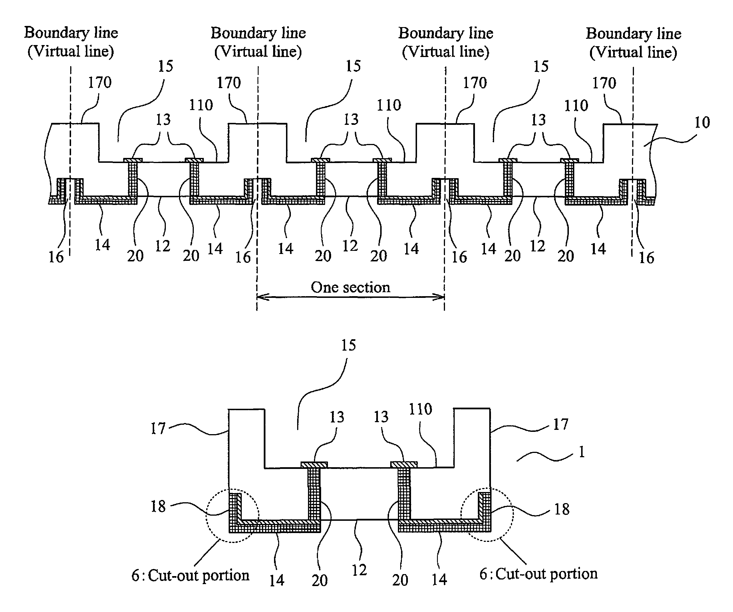
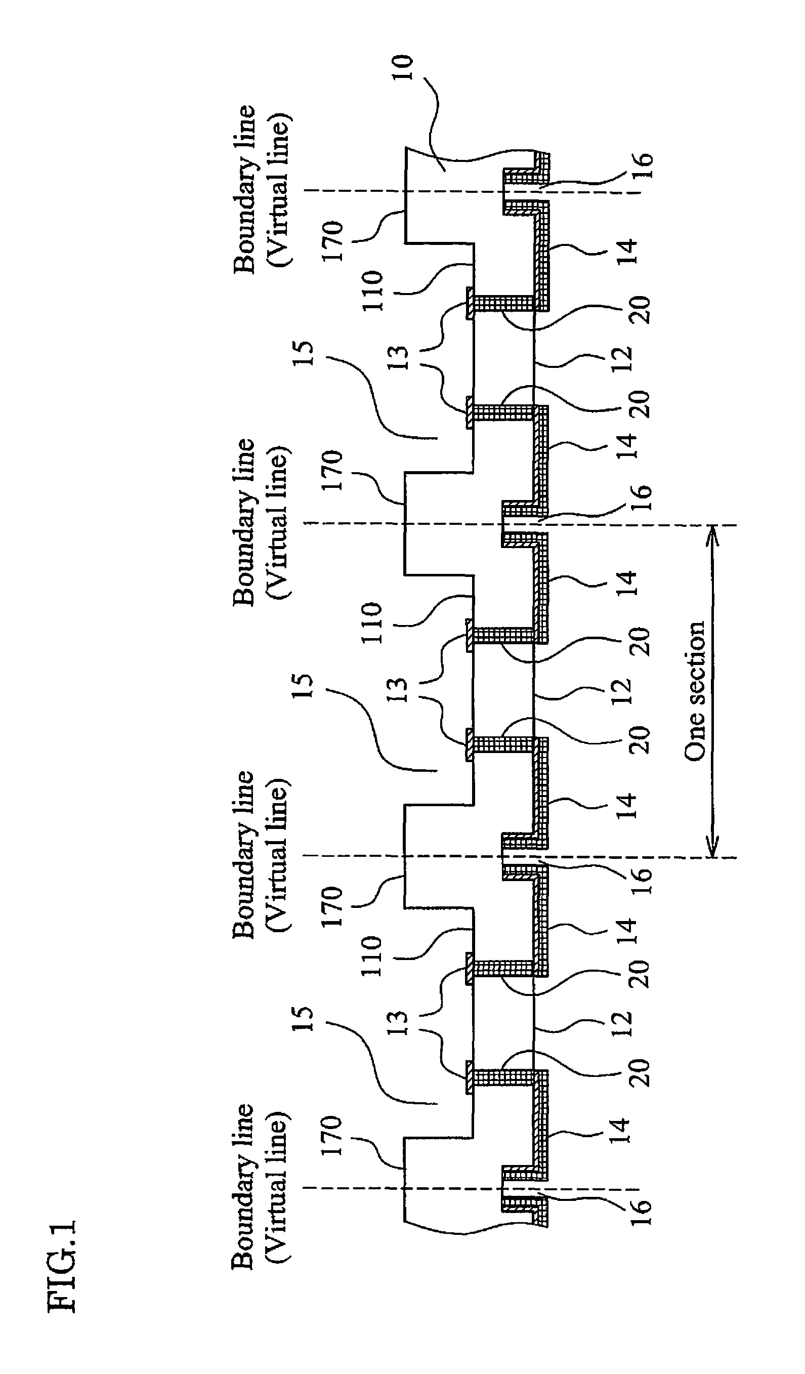
[0062]FIG. 1 is a schematic cross-sectional view of a package member assembly according to the first embodiment. A package member assembly 10 is an assembly in which a plurality of package members 1 are integrally formed. Here, it is assumed that a region indicated as “one section” in FIG. 1 is a single package member 1 (see FIG. 2).
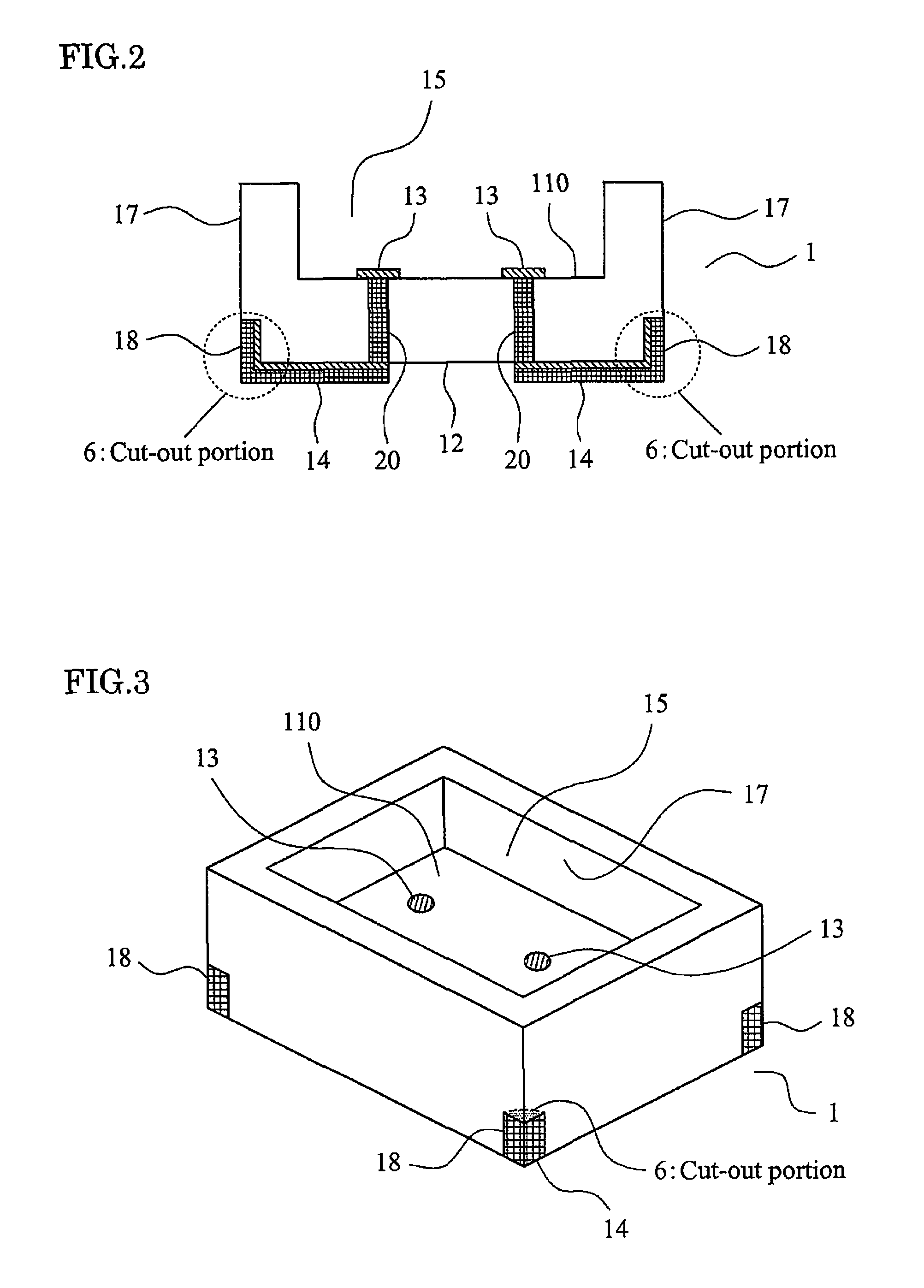
[0063]Next, a single package member 1 will be described with reference to FIGS. 2 and 3. FIG. 2 is a schematic cross-sectional view of the package member 1 according to the first embodiment. FIG. 3 is a perspective view of the package member 1 according to the first embodiment. The package member 1 is made of glass such as borosili...
second embodiment
[0103]Hereinafter, a second embodiment of the present invention will be described. Here, the same portions of the configuration as those in the first embodiment are not described, and have the same effects as those in the first embodiment. FIG. 19 is a schematic cross-sectional view of a crystal resonator 5′ according to the second embodiment.
[0104]The crystal resonator 5′ shown in FIG. 19 has, as main constituent elements, a crystal resonator plate 2′ that has a frame portion 28, and a package member 1′ and a lid 3′ (package member) that are bonded to the front and back of the crystal resonator plate 2′. The package member 1′ and the lid 3′ are bonded to front and back main faces 201 and 202 of the frame portion 28 of the crystal resonator plate 2′ via bonding materials 4 made of a brazing filler metal and a metal film. Here, in FIG. 19, Z-plate quartz crystal is used as base materials for the package member 1′ and the lid 3′.
[0105]The crystal resonator plate 2′ is an AT-cut crysta...
PUM
| Property | Measurement | Unit |
|---|---|---|
| conductive | aaaaa | aaaaa |
| shape | aaaaa | aaaaa |
| bond strength | aaaaa | aaaaa |
Abstract
Description
Claims
Application Information
 - R&D Engineer
- R&D Manager
- IP Professional
- Industry Leading Data Capabilities
- Powerful AI technology
- Patent DNA Extraction
Browse by: Latest US Patents, China's latest patents, Technical Efficacy Thesaurus, Application Domain, Technology Topic, Popular Technical Reports.
© 2024 PatSnap. All rights reserved.Legal|Privacy policy|Modern Slavery Act Transparency Statement|Sitemap|About US| Contact US: help@patsnap.com


