
Static random access memory devices having read and write assist circuits therein that improve read and write reliability

a random access memory and assist circuit technology, applied in static storage, information storage, digital storage, etc., can solve the problems of memory devices losing their stored data, reducing the stability of memory cells, and difficulty in the development of srams, so as to reduce the voltage of power supply signals

Active Publication Date: 2015-03-31
SAMSUNG ELECTRONICS CO LTD
View PDF6 Cites 20 Cited by
  • Summary
  • Abstract
  • Description
  • Claims
  • Application Information

AI Technical Summary

Benefits of technology

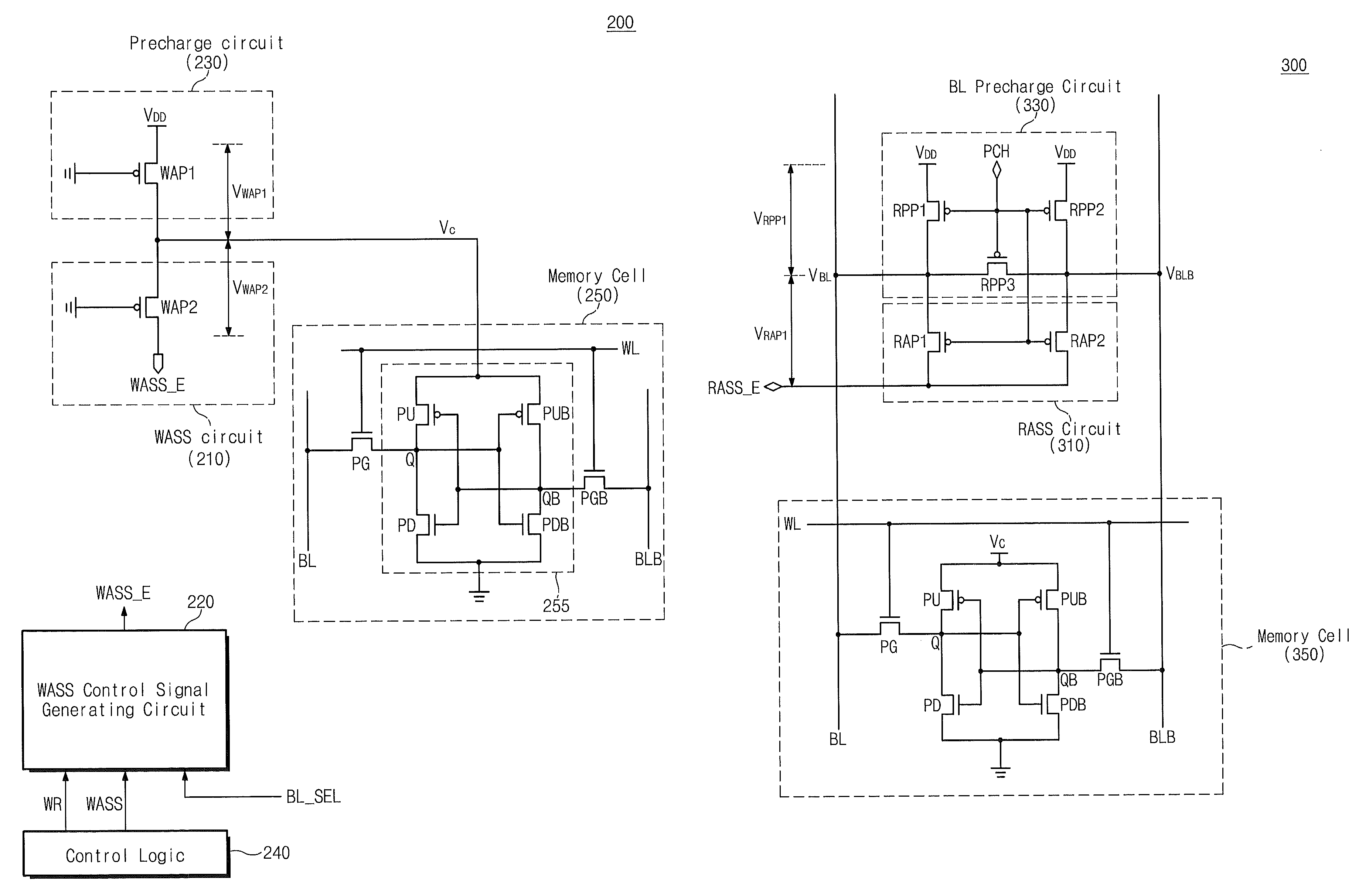
The invention is about a new type of integrated circuit memory that has a write assist circuit to help speed up the process of writing data to the memory. The write assist circuit reduces the power supply signal to the memory cell to a lower level, while the read assist circuit prepares the memory cell to read data by partially discharging the bit line. The memory cell is a specific type of static random access memory (SRAM) cell that uses a pair of PMOS push-up transistors. The invention also includes a method for writing and reading data to the SRAM cell. The new features improve the speed and reliability of the integrated circuit memory.

Problems solved by technology

Volatile memory devices lose their stored data when their power supplies are interrupted, while nonvolatile memory devices retain their stored data even when their power supplies are interrupted.
As semiconductor manufacturing processes become finer, the increased distribution leads to difficulty in development of SRAMs and reduction in stability of memory cells.

Method used


Image

  • Static random access memory devices having read and write assist circuits therein that improve read and write reliability
  • Static random access memory devices having read and write assist circuits therein that improve read and write reliability
  • Static random access memory devices having read and write assist circuits therein that improve read and write reliability

Examples


Embodiment Construction

[0019]The advantages and features of the inventive concept and methods of achieving them will be apparent from the following exemplary embodiments that will be described in more detail with reference to the accompanying drawings. It should be noted, however, that the inventive concept is not limited to the following exemplary embodiments, and may be implemented in various forms. Accordingly, the exemplary embodiments are provided only to disclose the inventive concept and let those skilled in the art know the category of the inventive concept. In the drawings, embodiments of the inventive concept are not limited to the specific examples provided herein and may be exaggerated for clarity. Furthermore, the same reference numerals denote the same elements throughout the specification. As used herein, the term “and / or” includes any and all combinations of one or more of the associated listed items. It will be understood that when an element is referred to as being “connected” or “couple...


PUM


Abstract

Integrated circuit memory devices include a memory cell configured to receive a power supply signal and a write assist circuit. The write assist circuit is configured to improve write margins by reducing a magnitude of the power supply signal supplied to the memory cell from a first voltage level to a lower second voltage level during an operation to write data into the memory cell. The memory device further includes at least one bit line electrically coupled to the memory cell and a read assist circuit. The read assist circuit may be configured to improve read reliability by partially discharging the at least one bit line from an already precharged voltage level to a lower third voltage level in preparation to read data from the memory cell.

Description

REFERENCE TO PRIORITY APPLICATION[0001]This U.S. non-provisional patent application claims priority under 35 U.S.C. §119 to Korean Patent Application No. 10-2010-0069002, filed Jul. 16, 2010, the entirety of which is hereby incorporated herein by reference.BACKGROUND[0002]Semiconductor memory device are typically classified into volatile memory devices and nonvolatile memory devices. Volatile memory devices lose their stored data when their power supplies are interrupted, while nonvolatile memory devices retain their stored data even when their power supplies are interrupted.[0003]Volatile memory devices include static random access memories (SRAMs) and dynamic random access memories (DRAMs), which are roughly categorized according to data storage schemes. That is, an SRAM stores data by using a latch while a DRAM stores data by using a capacitor. Especially, an SRAM is mainly used as a cache memory because its peripheral circuit is simple in configuration and its speed is high in s...

Claims


Application Information

Patent Timeline
Patent Type & Authority Patents(United States)
IPC IPC(8): G11C7/22G11C11/413
CPCG11C11/413G11C5/14G11C7/12G11C11/5642
Inventor JUNG, JONGHOONSIM, SOUNGHOON
Owner SAMSUNG ELECTRONICS CO LTD
Learn More