
Fixed-outline floorplanning approach for mixed-size modules

a floorplaning and mixed-size technology, applied in the direction of multi-objective optimization, program control, instruments, etc., can solve the problems of not only taking longer execution time, not only able to change the aspect ratio, and not only able to achieve full automation in this regard, so as to shorten the design time of ic design flow, enhance chip performance, and save the wire-length of the chip

Inactive Publication Date: 2015-02-24
NAT CHENG KUNG UNIV
View PDF46 Cites 2 Cited by
  • Summary
  • Abstract
  • Description
  • Claims
  • Application Information

AI Technical Summary

Benefits of technology

The present invention provides a fixed-outline floorplanning approach for mixed-size modules. The approach involves evenly distributing circuit modules over chip area, generating a slicing tree, and removing overlap between circuit modules to save wire-length and improve chip performance. Compared to traditional floorplanning methods, the present invention achieves stable results in quick time and improves average wire-length.

Problems solved by technology

Because it is manually drafted by engineers, its aspect ratio cannot be changed.
In other words, full automation in this regard is not available.
Because the simulated annealing algorithm is non-deterministic, it not only takes longer execution time, but also obtains different results in each time.
Although DeFer is efficient and effective, it has two major disadvantages as follows: (1) it can obtain good result while only wire-length is considered.
That is, DeFer is hard to be extended to consider other factors such as thermal and routability, which are important issues in modern designs.

Method used


Image

  • Fixed-outline floorplanning approach for mixed-size modules
  • Fixed-outline floorplanning approach for mixed-size modules
  • Fixed-outline floorplanning approach for mixed-size modules

Examples


Embodiment Construction

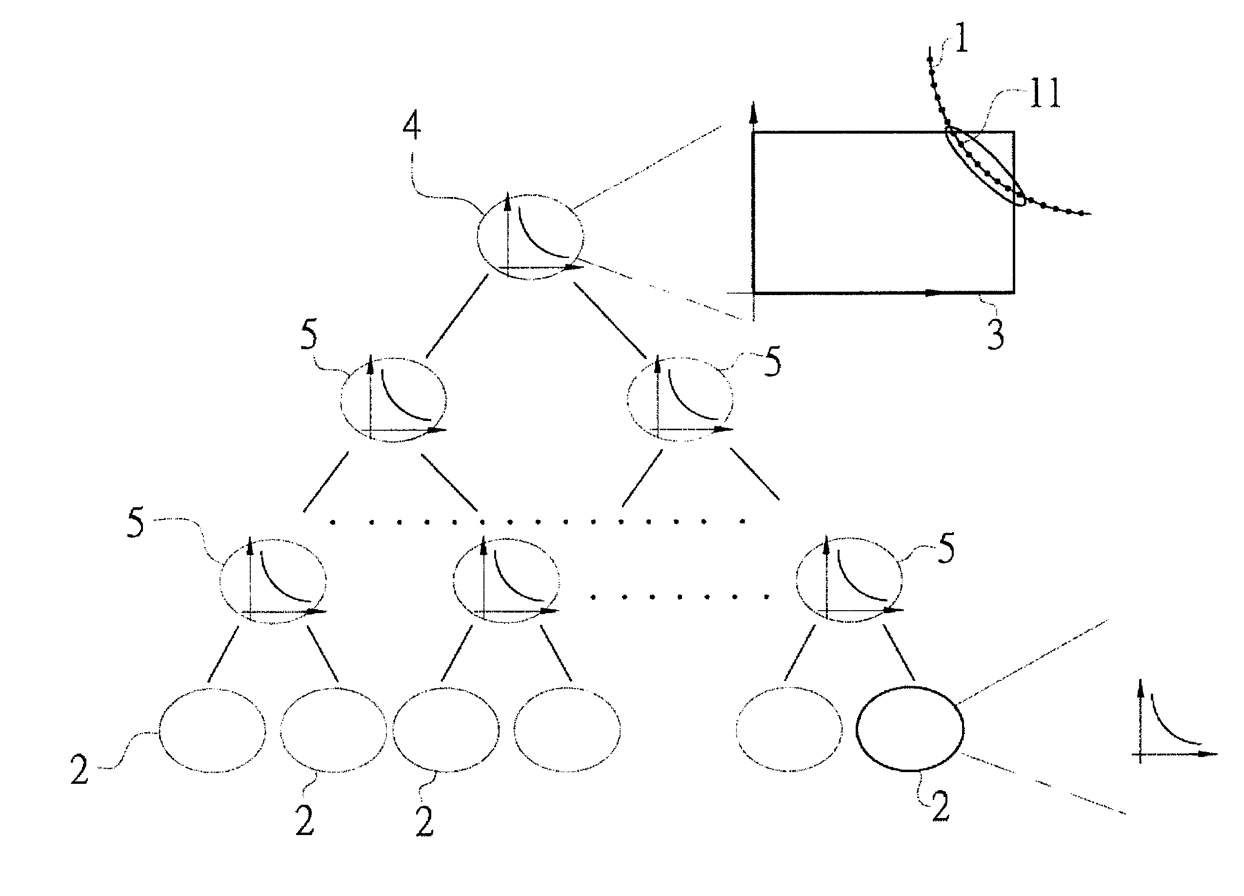
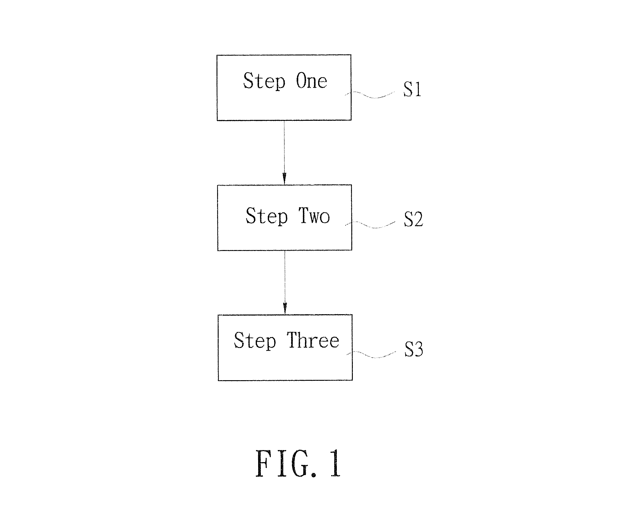
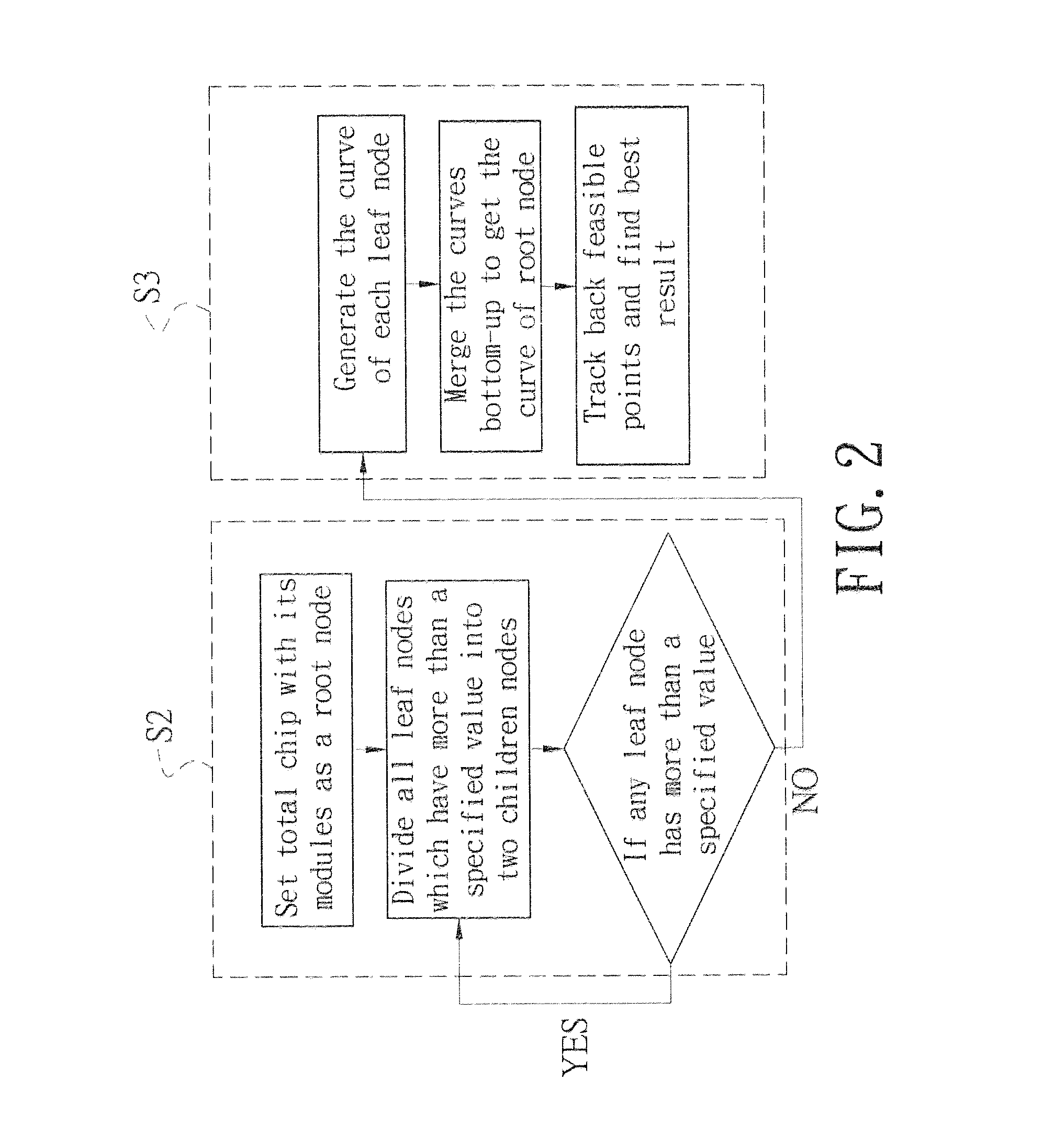
[0021]First refer to FIG. 1 for a floorplanning approach for mixed-size modules according to the present invention. It handles fixed-outline driven floorplanning for mixed-size circuit modules which include soft modules and hard modules. A hard module usually refers to a customized module which has fixed width and height (e.g. analog circuit modules), and a soft module denotes a digital module with a fixed area, in which the aspect ratio of its outline can be changed arbitrarily within a predefined range. The floorplanning approach includes following steps.

[0022]Step one (S1): evenly distributing circuit modules including hard modules and soft modules over whole chip area, which is called a global distribution stage. The analytical based approach or force directed approach can be applied. The objective of the force directed approach is the curve path with the least consumed energy when optimization of every circuit module placement. The analytical based approach is to compute wire-l...


PUM


Abstract

A fixed-outline floorplanning approach for mixed-size modules is disclosed. Firstly, evenly distribute mixed-size circuit modules to whole chip area based on different requirements such as wire-length, routability, or thermal in the global distribution stage. To maintain the global distribution result and satisfy the fixed-outline constraint, generate a slicing tree by recursively applying partition algorithm to divide modules distributed in a given region into several sub-regions. Then, to remove overlap between circuit modules and find a best solution, use bottom-up shape curve merging and top-down back tracing procedure to generate a slicing tree. The shape curve for each leaf in the tree is built first by enumerated packing. Then, the curves in the tree are merged iteratively from bottom to top, and feasible solutions in the shape curve of the root node are identified according to the fixed-outline constraint. Finally, the best solution is determined by a top-down back tracing procedure.

Description

BACKGROUND OF THE INVENTION[0001]1. Fields of the Invention[0002]The present invention relates to a fixed-outline floorplanning approach for mixed-size modules, especially by means of evenly distributing circuit modules over a chip outline in the global distribution stage based on different requirements, such as wire-length, thermal, routability, performance and so on, and removing the overlap between circuit modules in a legalization stage without violating relative positions of the modules determined in the global distribution results and the fixed-outline constraint, so as to save the wire-length of the chip, enhance the chip performance and shorten the time of IC design flow.[0003]2. Descriptions of Related Art[0004]Floorplanning, which determines the shapes and locations of modules in a chip, is an important step in VLSI design, and chip performance is deeply affected by the results. In order to reduce design complexity, hierarchical designs are widely applied approaches on SoC...

Claims


Application Information

Patent Timeline
Patent Type & Authority Patents(United States)
IPC IPC(8): G06F17/50
CPCG06F17/5072G06F17/5081G06F30/392G06F2111/06G06F30/398
Inventor LIN, CHIA-MINCHAN, KAI-CHUNG
Owner NAT CHENG KUNG UNIV
Learn More