Opto-electric device and method of manufacturing thereof

a technology of opto-electric devices and manufacturing methods, applied in the direction of solid-state devices, semiconductor devices, organic semiconductor devices, etc., can solve the problems of inhomogeneous light emission, inability to increase the thickness of the transparent electrode layer too much, unacceptably low transparency, etc., and achieve the effect of efficient manufacturing and efficient manufacturing methods

Inactive Publication Date: 2015-02-24
NEDERLANDSE ORG VOOR TOEGEPAST NATUURWETENSCHAPPELIJK ONDERZOEK TNO
View PDF21 Cites 5 Cited by
  • Summary
  • Abstract
  • Description
  • Claims
  • Application Information

AI Technical Summary

Benefits of technology

[0012]It is a purpose of the invention to provide a more efficient method to manufacture an opto-electric device, as well as an opto-electric device that can be manufactured more efficiently.
[0029]Dependent on the temperature range wherein the opto-electric device is used and the temperature range allowed by the opto-electric layer the skilled person may select the most suitable metal or metal alloy from a variety of metals and metal alloys. For example the skilled person may select for example from commercially available, low cost, low-melting metals and metal alloys. These may comprise for example elements selected from the group consisting of In, Sn, Bi, Pb, Hg, Ga and Cd. Apart from a broad spectrum of melting points, said metals also offer a broad spectrum of other properties which are important, such as sensitivity to oxidation, adhesion to other materials, coefficient of thermal expansion, ductility, dimensional stability, degree of shrinkage upon solidification and wetting. In applications in which toxicity is an important factor, alloys containing Hg or Cd, such as Sn: (50 wt. %): Pb (32 wt. %): Cd (18 wt. %) alloy are not to be preferred. If a somewhat flexible EL device is necessary, it is advantageous to use a ductile low-melting metal, such as indium (melting point 157 C) or Sn (35.7 wt. %): Bi (35.7 wt. %): Pb (28.6 wt. %), which has a melting point of 100 C. To minimize stresses caused by solidification, a metal which, upon solidification, does not form crystalline domains and exhibits little shrinkage, such as Bi (58 wt. %): Sn (42 wt. %), melting point 138 C, is preferred.
[0040]In a particular embodiment, the suspension or colloidal solution may be printed in a narrow line structure if the surface of the opto-electric layer is prepared with a surface energy modifying agent. Dependent on the surface energy in of the surface where the suspension or colloidal solution is applied, contact angles in the range of 30 deg to 60 deg may be realized. The inkjet printer used may eject the substance to be printed in the form of drops that merge into a continuous pattern, or may print a continuous beam of the substance to be printed at the surface. In an embodiment the process of printing is repeated. Therewith a relative high aspect ratio (height / width ratio) of the printed pattern can be achieved.
[0058]The electron transport, layer can function both to facilitate electron transport, and also serve as a buffer layer or confinement layer to prevent quenching of the exciton at layer interfaces. Preferably, this layer promotes electron mobility and reduces excitors quenching. Examples of electron transport materials which can be used in the optional electron transport layer, include metal chelated oxinoid compounds, including: metal quinolate derivatives such as tris(8-hydroxyquinolato)aluminum (AIQ), bis(2-methyl-8-quinolinotato)(p-phenylphenolato) aluminum (BAN), tetrakis-(8-hydroxyquinolato)hafnium (HfQ) and tetrakis-(8-hydroxyquinolato)zirconium (ZrQ); and azole compounds such as 2-(4-biplienyiyl)-5˜(4-t-butylphenyl)-1,3,4-oxadiazole (PBD), 3-(4-biphenylyl)-4-phenyl-5-(4-t-butylphenyl)-1,2,4-triazole (TAZ), and 1,3,5-tri(phenyl-2-benzimidazole)benzene (TPBI); quinoxaltne derivatives such as 2,3-bis(4-fluorophenyl)quinoxaline; phenanthrotines such as 4,7˜diphenyl-1,10˜phenanthroline (DPA) and 2,9-dimethyl-4,7-diphenyl-1,10-phenanthroline (DDPA); and mixtures thereof.

Problems solved by technology

The present thin film materials used for the semitransparent electrode (e.g. ITO) have a large resistivity and the large currents give rise to a substantial voltage drop, which results in inhomogeneous light emission.
However, the thickness of the transparent electrode layer cannot be increased too much in order to avoid an unacceptably low transparency.

Method used


Image

  • Opto-electric device and method of manufacturing thereof
  • Opto-electric device and method of manufacturing thereof
  • Opto-electric device and method of manufacturing thereof

Examples


Embodiment Construction

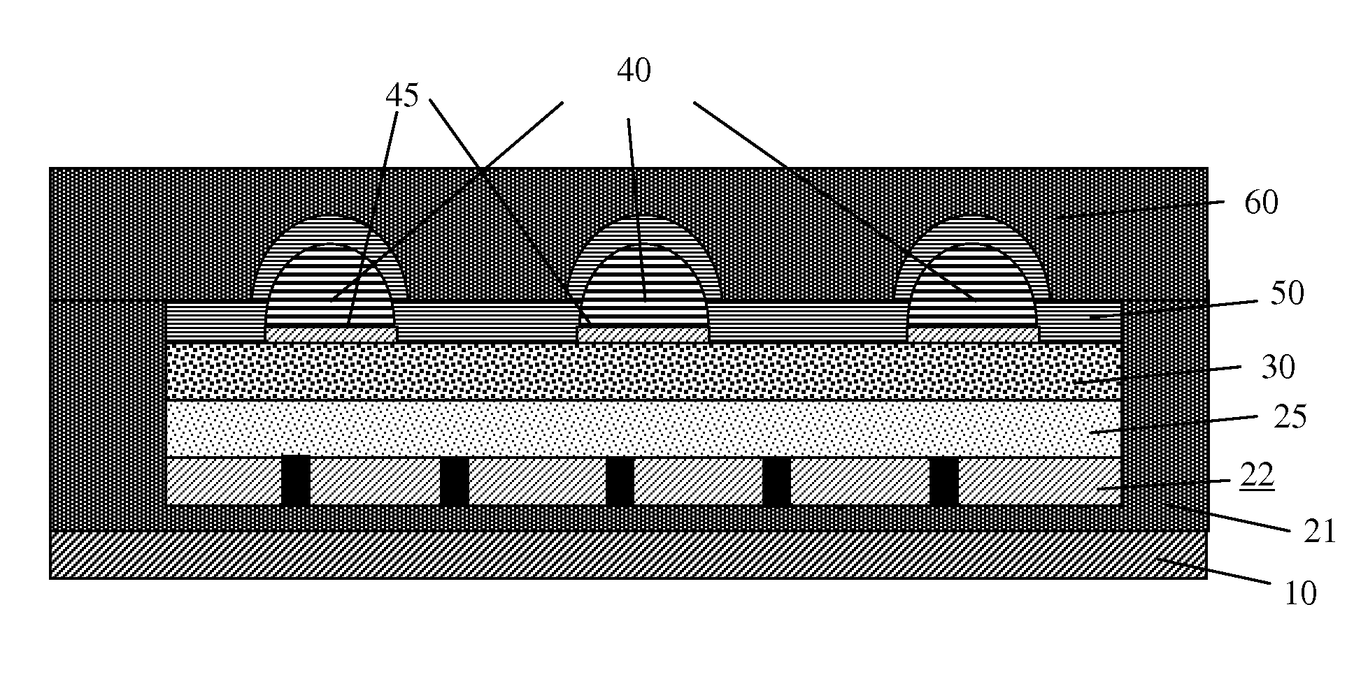
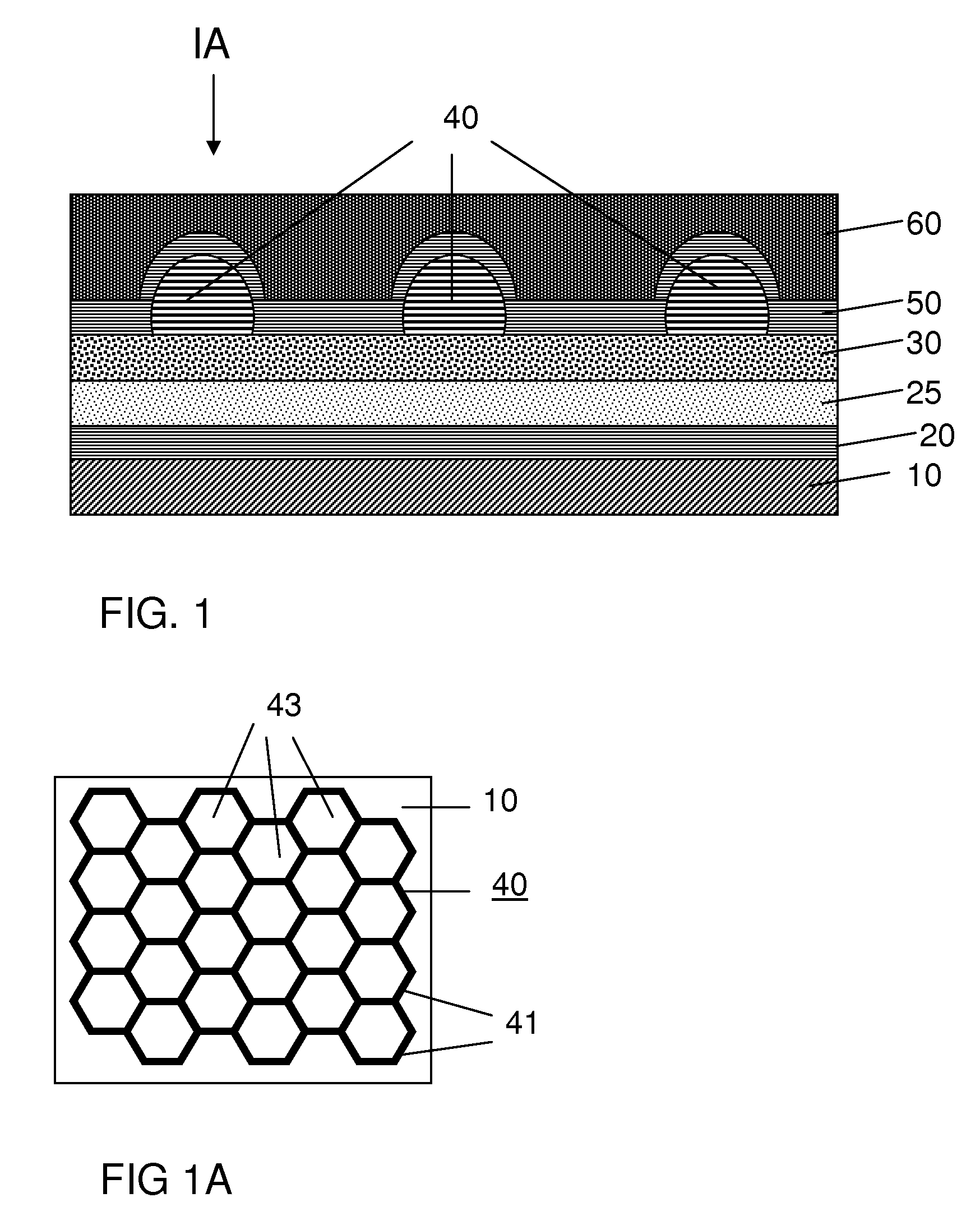
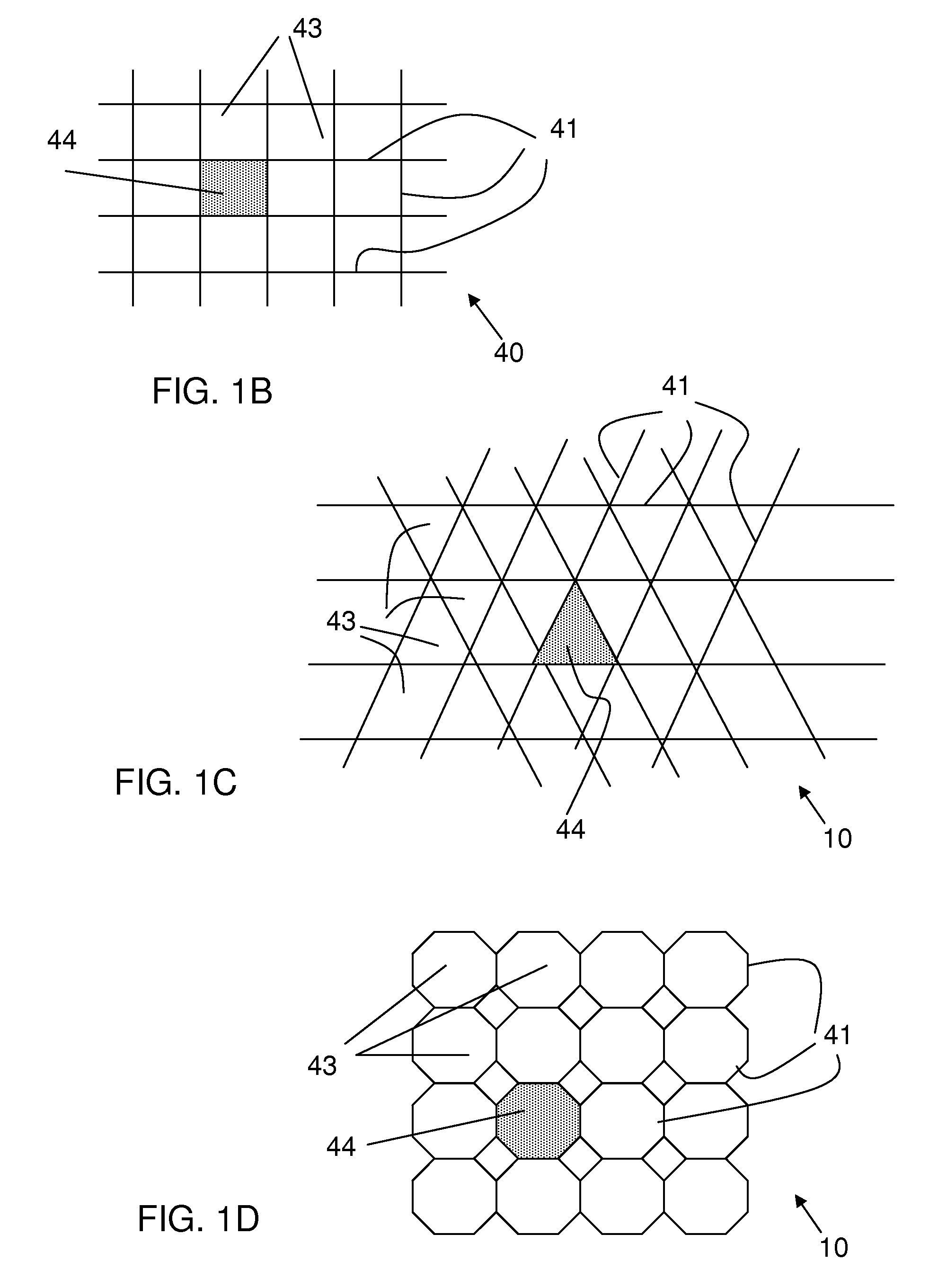
[0084]In the following detailed description numerous specific details are set forth in order to provide a thorough understanding of the present invention. However, it will be understood by one skilled in the art that the present invention may be practiced without these specific details. In other instances, well known methods, procedures, and components have not been described in detail so as not to obscure aspects of the present invention.

[0085]In the drawings, the size and relative sizes of layers and regions may be exaggerated for clarity.

[0086]It will be understood that, although the terms first, second, third etc. may be used herein to describe various elements, components, regions, layers and / or sections, these elements, components, regions, layers and / or sections should not be limited by these terms. These terms are only used to distinguish one element, component, region, layer or section from another region, layer or section. Thus, a first element, component, region, layer or...


PUM


Abstract

The present invention relates to an opto-electric device having a stack of layers subsequently comprisinga first electrode layer (20) of a material having a first work function, deposited on a substrate (10) or forming a substrate (20),an organic opto-electric layer (30) on the first electrode layer (20),a patterned electrically conductive layer (40) printed on the opto-electric layer (30),a transparent, second electrode layer (50) of a material having a second work function on the opto-electric layer (30) provided with the patterned electrically conductive layer (40), the second work function having a value lower than the first work function.

Description

CROSS-REFERENCE TO RELATED APPLICATIONS[0001]This application is a U.S. National Stage application under 35 U.S.C. §371 of International Application PCT / NL2011 / 050438 (published as WO 2011 / 159160 A1), filed Jun. 17, 2011, which claims priority to Application EP 10166379.7, filed Jun. 17, 2010. Benefit of the filing date of each of these prior applications is hereby claimed. Each of these prior applications is hereby incorporated by reference in its entirety.BACKGROUND OF THE INVENTION[0002]1. Field of the Invention[0003]The present invention relates to an opto-electric device.[0004]The present invention further relates to a method of manufacturing an opto-electric device.[0005]2. Related Art[0006]An opto-electric device is a device that provides for an optical effect in response to an electric signal, or that generates an electric signal in response to an optical stimulus. Examples of the first are light emitting diodes, such as organic light emitting diodes. Nowadays various photoa...

Claims


Application Information

Patent Timeline
Patent Type & Authority Patents(United States)
IPC IPC(8): H01L33/00H01L33/36H01L51/50H01L51/52H01L51/56
CPCH01L51/5203H01L51/5221H01L33/36H01L51/56H01L51/5092H01L2251/5315H10K50/171H10K50/824H10K50/828H10K2102/3026H10K50/805H10K50/82H10K2102/351H10K71/00
Inventor HERMES, DOROTHEE CHRISTINEWILSON, JOANNE SARAH
Owner NEDERLANDSE ORG VOOR TOEGEPAST NATUURWETENSCHAPPELIJK ONDERZOEK TNO
Why Eureka
Try Eureka