Dynamic random access memory device with improved control circuitry for the word lines

a memory device and dynamic random access technology, applied in the direction of digital storage, electrical equipment, instruments, etc., can solve the problem of nmos transistors oxidizing after two days and a few hours, and achieve the effect of reducing the risk of oxide breakdown and high working frequency

Inactive Publication Date: 2014-12-02
STMICROELECTRONICS (CROLLES 2) SAS
View PDF10 Cites 0 Cited by
  • Summary
  • Abstract
  • Description
  • Claims
  • Application Information

AI Technical Summary

Benefits of technology

[0005]According to one embodiment, a memory device may reduce the risk of oxide breakdown, i.e. TDDB, of NMOS transistors while applying to the word lines to be selected, significant voltages greater than the admissible voltage of the NMOS transistors, thus making it possible to obtain high working frequencies, for example of the order of 550 MHz.
[0013]To reduce the effects due to hot carrier injections, known to the person skilled in the art by the acronym “HCI”, which may appear in the presence of a high source-drain voltage when a MOS transistor conducts, and which induce defects in the gate leading to degradations of the transistor, in one embodiment, the second level-translator stage may comprise a second PMOS transistor pair having their gate coupled to the first voltage-elevator stage and connected in series between the PMOS transistors of the first pair and the group of NMOS transistors.

Problems solved by technology

Thus, by way of indication, in a 32-nanometer technology, the application of 2.5 volts to the selected word lines of the memory plane may lead to oxide breakdown of the NMOS transistors after two days and a few hours.

Method used


Image

  • Dynamic random access memory device with improved control circuitry for the word lines
  • Dynamic random access memory device with improved control circuitry for the word lines
  • Dynamic random access memory device with improved control circuitry for the word lines

Examples


Embodiment Construction

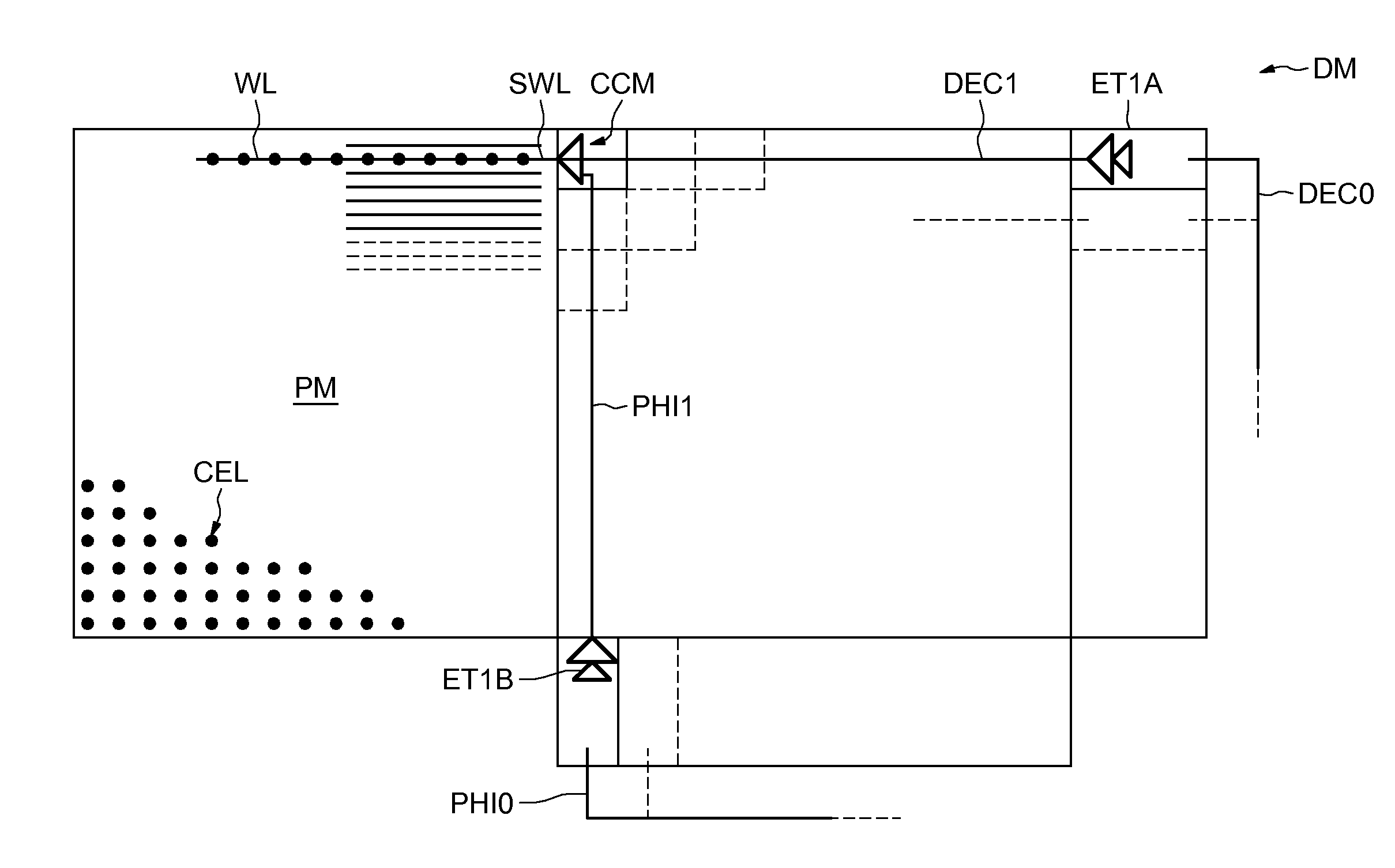
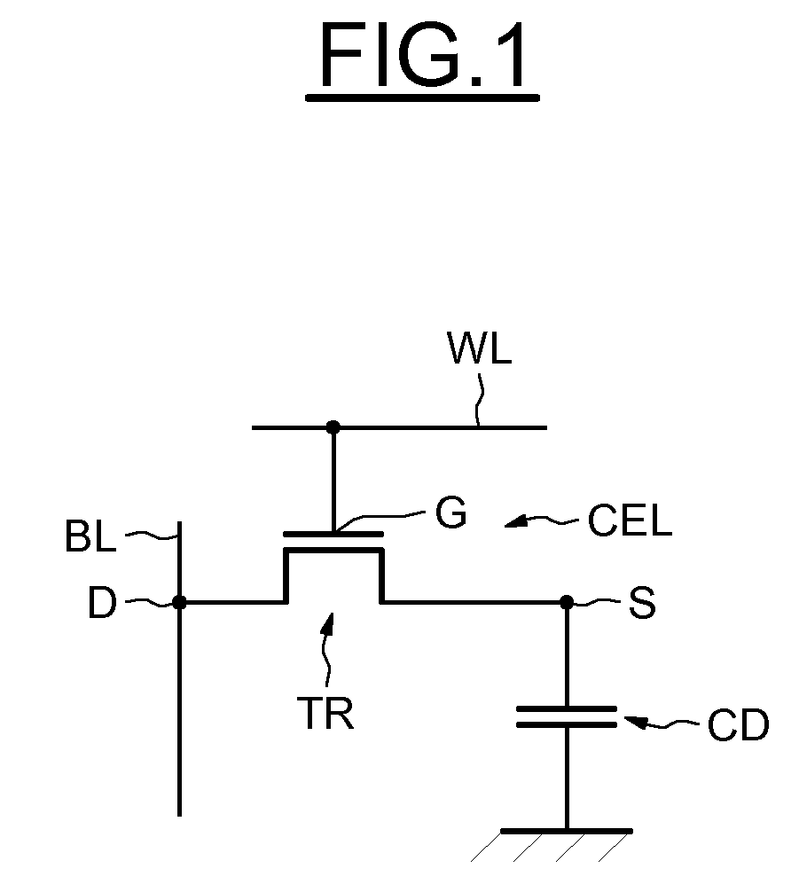
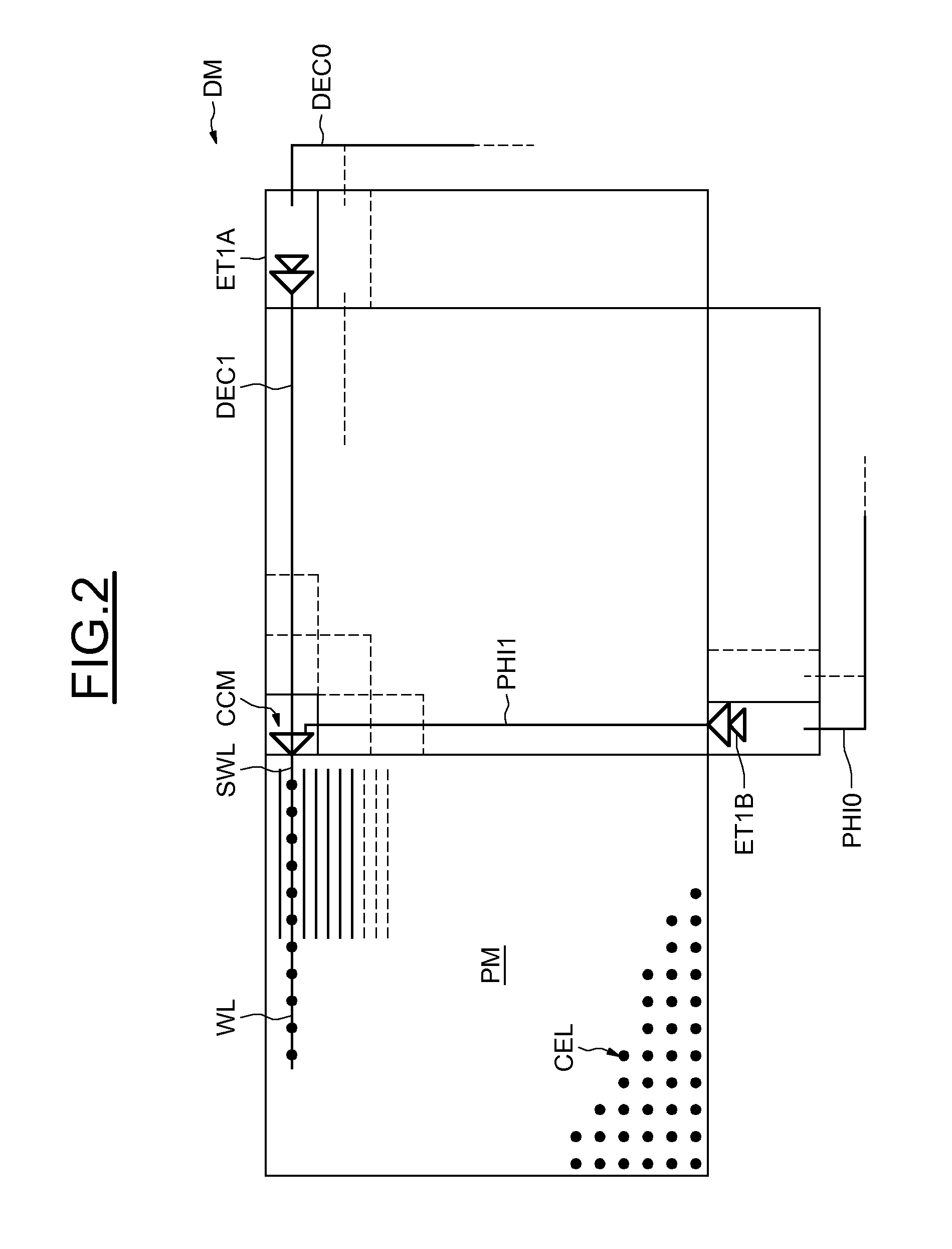
[0018]In FIG. 1, the reference CEL designates a DRAM memory cell comprising, in a conventional manner, an access transistor TR whose gate G is linked to a word line WL, whose drain D is connected to a bit line BL and whose source S is connected to a storage capacitor CD. Access transistors TR having threshold voltages VT sufficiently high to reduce charge leakage are preferably chosen. Thus for example, dual-oxide transistors, well known to the person skilled in the art, having threshold voltages of the order of 1 volt may be needed.

[0019]Moreover, in the case where the nominal supply voltage of the bit line is of the order of 1 volt, this being the case in 32-nanometer technologies, it is generally desirable to apply a voltage of the order of 2.5 volts to the gate of the transistor TR to have a gate-source voltage much greater than the threshold voltage, and thus have a relatively short write time. Thus, it may ultimately be possible to obtain a high working frequency for the memor...


PUM


Abstract

A dynamic random access memory device may include DRAM memory cells including several lines of memory cells, and line selection circuitry associated with each line. The line selection circuitry may include a first voltage-elevator stage configured to receive two initial control logic signals each having an initial voltage level corresponding to a first logic state, and to deliver two intermediate control logic signals each having an intermediate voltage level above the initial level and corresponding to the first logic state. The line selection circuitry may also include a control circuit to be supplied by PMOS transistors with a supply voltage having a second voltage level greater than the intermediate voltage level, and configured to, in the presence of the two intermediate control logic signals have their first logic state deliver to the gates of the memory cell transistors, a selection logic signal having the second voltage level.

Description

FIELD OF THE INVENTION[0001]The invention relates to dynamic random access memory devices known to the person skilled in the art by the acronym “DRAM”, and, more particularly, to the control circuitry for the word lines of the memory plane.BACKGROUND OF THE INVENTION[0002]In a writing operation to a DRAM memory cell it may be desirable to apply a high voltage to the word line to which the cell is connected, so as to have a high gate-source voltage at the level of the cell's access transistor. This may allow, in particular, writing under good conditions while offering a relatively high refresh frequency. Thus, by way of indication, for advanced technologies, for example, technologies below 45 nanometers, in particular, 32 nanometers, obtaining a refresh frequency of 550 MHz may make it desirable to apply a line selection signal (voltage) of 2.5 volts to the word line.[0003]Moreover, the generation of the line selection signal may be obtained based upon a combination of two control si...

Claims


Application Information

Patent Timeline
Patent Type & Authority Patents(United States)
IPC IPC(8): G11C8/08G11C11/408G11C5/14H01L21/50G11C7/00
CPCG11C7/00H01L21/50G11C8/08G11C11/4085G11C11/4087
Inventor JEANTET, OLIVIERVERNET, MARC
Owner STMICROELECTRONICS (CROLLES 2) SAS
Why Eureka
Try Eureka