
Method and apparatus of physical property measurement using a probe-based nano-localized light source

a nano-localized light source and physical property technology, applied in the direction of nanotechnology, measurement devices, instruments, etc., can solve the problems of limited chemically specific information, reduced sensitivity, and difficult simultaneous spectroscopic implementation of delivering chemical specificity and sensitivity on the molecular level, so as to facilitate optically making physical property measurements on a sample, the separation of the tip is small, and the separation of the tip is less.

Inactive Publication Date: 2014-11-04
BRUKER NANO INC
View PDF14 Cites 9 Cited by
  • Summary
  • Abstract
  • Description
  • Claims
  • Application Information

AI Technical Summary

Benefits of technology

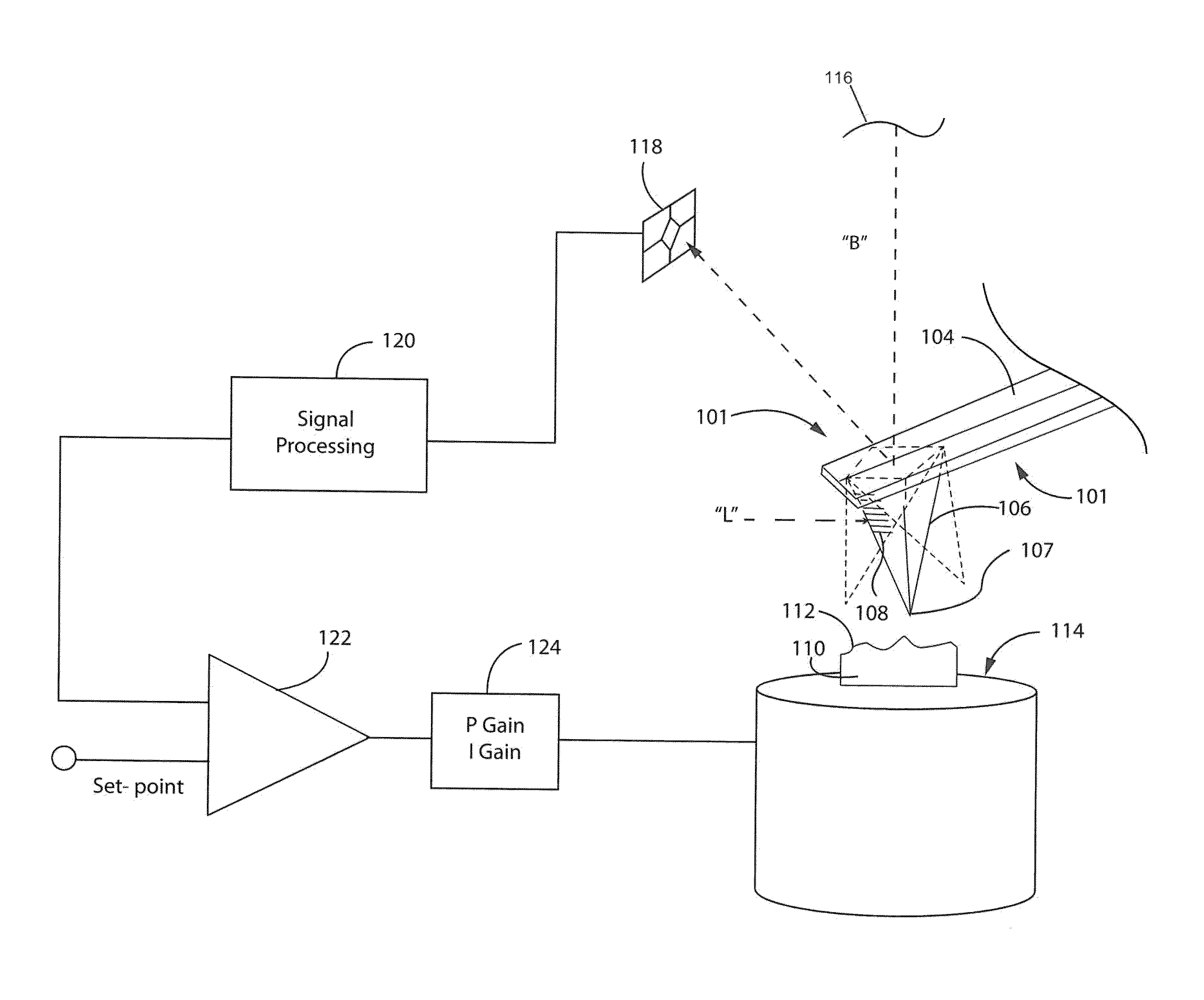
[0023]Efficiency of optically making physical property measurements on a sample is facilitated by employing a combination of an atomic force microscope (AFM) capable of maintaining a tip-sample separation sufficiently small with SPM tips designed with a unique geometry (e.g., waveguide) that can be used to transform a quasi-planar SPP mode coupled via a receiving element into a spatially confined excitation source. In a preferred embodiment, the so-called torsional resonance mode (TR Mode) may be used to maintain tip-sample separation less than. 100 nm, though Tapping Mode AFM using low amplitude oscillation may also be employed. Combined with the described antenna concept, the preferred embodiments provide highly efficient generation of nano-localized excitations with an inherently broad operational bandwidth and only a weak wavelength dependence. In a scanning probe microscope, this allows for nearly background-free s-SNOM imaging with any spectroscopic techniques, and associated chemical specificity. The preferred embodiments are usable in spectroscopy set-ups, as well as in nano-imaging applications employing a set wavelength.
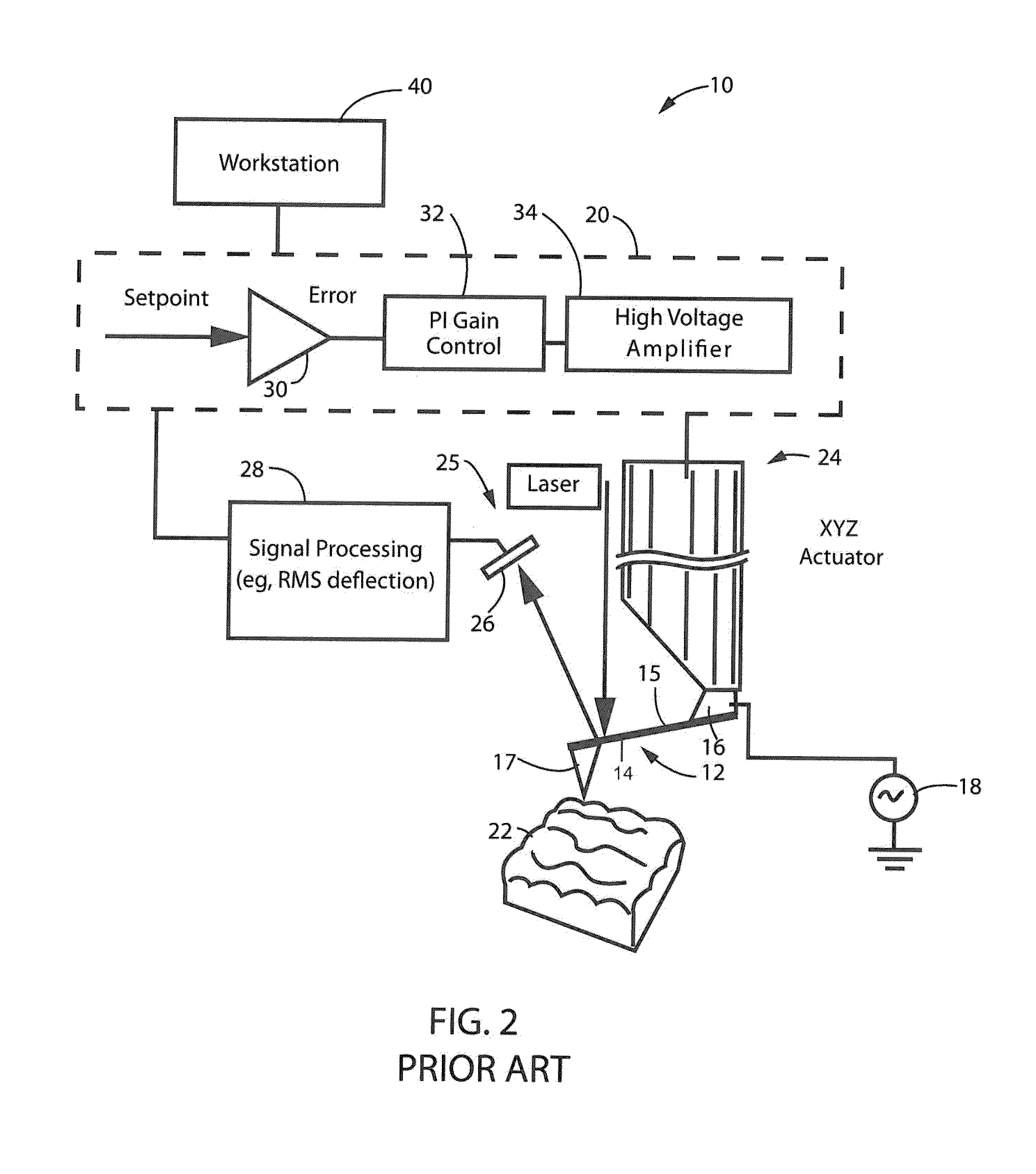
[0024]In the present preferred embodiments, an SPM probe includes a cantilever and a tip, with the tip positioned at the distal end of the cantilever, and including a) a shaft and b) an apex positioned adjacent to a sample. A receiving element is provided and supported by the shaft of the tip. A source of electromagnetic wave excitation directs electromagnetic waves toward the receiving element, the electromagnetic wave being coupled to the apex via the receiving element. The coupled electromagnetic excitation at the apex is locally enhanced and interacts with the sample. A controller maintains a separation between the apex and the sample greater than zero nanometers and less than 100 nm during electromagnetic wave excitation.

Problems solved by technology

But, as noted by Berweger et al, in Adiabatic Tip-plasmon Focusing for Nano-Raman Spectroscopy, J. Phys. Chem. Letters (November 2010) (“Berweger I”), the entirety of which is hereby incorporated by reference, despite ongoing progress in the development of imaging techniques with spatial resolution beyond the diffraction limit, simultaneous spectroscopic implementations delivering chemical specificity and sensitivity on the molecular level have remained challenging.
Far-field localization techniques can achieve spatial resolution down to about 20 nm by point-spread function reconstruction, but typically rely on fluorescence from discrete molecular or quantum dot emitters, with limited chemically specific information.
However, aperture-limited and wavelength-dependent fiber throughput reduces sensitivity, generally making SNOM unsuitable for spectroscopic techniques that have low intrinsic signal levels.
In the standard implementation, however, the direct illumination of the tip apex results in a three-to-four orders of magnitude loss in excitation efficiency, related to the mode mismatch between the diffraction-limited far-field excitation focus and the desired tens of nanometers near-field localization, as determined by the tip apex radius.
The resulting loss of sensitivity, together with a far-field background signal, often limit contrast and may cause imaging artifacts, presenting challenges for the general implementation of a wider range of spectroscopic techniques in s-SNOM.
While this can be achieved through a nanoscopic emitter in the form of a single molecule, quantum dot, or nano structure at the apex of a tip, that approach relies on the quantum efficiency and spectral characteristics of the emitter, and the difficulties of overcoming the intrinsic background and sensitivity limitations with unmatched far-field mode excitation remain.
As explained by the authors, it was believed that the geometric constraints of the cantilever-based design made the study of opaque samples difficult, and the collinear excitation and residual hole-array transmission did not yet fully eliminate the far-field background.
But such known systems have limitations.
For example, the tip-sample coupling relationship is complex and can, for example, result in a loss of excitation enhancement due to the broad k-vector distribution at the apex allowing for launching propagating SPPs at the sample surface.
Also, use of electrochemically etched tips is limited to shear force microscopy (tuning fork tips—difficult to implement tip-sample modulation with these).
As a result, the AFM modes available for simultaneous and sensitive topographic, phase, and other state of the art AFM functions is severely limited.
Electrochemically etched tips are also difficult to mass produce, and their reproducibility is limited.
In addition, the materials that can be used to produce the tips are limited.

Method used


Image

  • Method and apparatus of physical property measurement using a probe-based nano-localized light source
  • Method and apparatus of physical property measurement using a probe-based nano-localized light source
  • Method and apparatus of physical property measurement using a probe-based nano-localized light source

Examples


Embodiment Construction

[0054]An improved apparatus and method of performing nano-image and spectroscopic measurements efficiently and locally on the nanoscale is shown and described. In one embodiment, sharp tipped probes employed in a conventional metrology instrument, such as an atomic force microscope (AFM), are configured to provide a top-down nano-localized light source. Rather than using far-field light which has a low density of states (essentially only one mode), the nano-localized light source of the preferred embodiments provides a localized optical dipole of high intensity. The concept is akin to Förster resonance energy transfer (FRET), which looks at the energy transfer from one excited dye molecule (chromophore) to another to measure distances between the molecules. In analogous fashion, the nano-localized light source employed in the preferred embodiments is used as on an SPM probe to provide highly efficient excitation of the sample, thus allowing the preferred embodiments to make spectros...


PUM


Abstract

An apparatus and method of performing physical property measurements on a sample with a probe-based metrology instrument employing a nano-confined light source is provided. In one embodiment, an SPM probe tip is configured to support an appropriate receiving element so as to provide a nano-localized light source that is able to efficiently and locally excite the sample on the nanoscale. Preferably, the separation between the tip apex and the sample during spectroscopic measurements is maintained at less than 10 nm, for example, using an AFM TR Mode control scheme.

Description

CROSS-REFERENCE TO RELATED APPLICATIONS[0001]This application claims priority under 35 USC §1.119(e) to U.S. Provisional Patent Application Ser. No. 61 / 775,166, filed Mar. 8, 2013, entitled Method and Apparatus of Physical Property Measurement Using a Probe-Based Nano-Localized Light Source. The subject matter of this application is hereby incorporated by reference in its entirety.BACKGROUND OF THE INVENTION[0002]1. Field of the Invention[0003]The preferred embodiments are directed to using a nano-localized light source to measure physical properties of a sample, and more particularly, to a method and apparatus of making nano-imaging and spectroscopy measurements using an atomic force microscope operating in either contact or a low amplitude mode, with the tip apex of the probe functioning as the nano-localized source.[0004]2. Description of Related Art[0005]The interaction between a sample under test and radiated energy can be monitored to yield information concerning the sample. I...

Claims


Application Information

Patent Timeline
Patent Type & Authority Patents(United States)
IPC IPC(8): G01Q60/00G01Q10/00
CPCG01Q60/22G01Q10/065B82Y35/00B82Y20/00G01Q60/06G01Q10/00G01Q20/02G01Q60/38
Inventor RASCHKE, MARKUS B.KAEMMER, STEFAN B.MINNE, STEPHEN C.SU, CHANMIN
Owner BRUKER NANO INC
Learn More