III-V photovoltaic elements

a photovoltaic element and absorber material technology, applied in the field of physical sciences, can solve the problems of not providing a platform for manufacturing high-efficiency cells, reducing the efficiency of solar cells, and reducing the cost of solar cells for many terrestrial applications. achieve the effect of improving the efficiency of carrier collection and improving the performance of solar cells

Inactive Publication Date: 2014-10-28
IBM CORP
View PDF4 Cites 1 Cited by
  • Summary
  • Abstract
  • Description
  • Claims
  • Application Information

AI Technical Summary

Benefits of technology

[0008]Techniques of the present invention can provide substantial beneficial technical effects, including methods of making high efficiency solar cells having particular utility in solar panels. The resulting structures can, however, be used for energy autonomous solar-powered electronic circuits and sensors. One or more embodiments may provide one or more of the following advantages:[0009]Improving open circuit voltage (Voc)[0010]Improving the short circuit current density (Jsc)[0011]Improving solar cell efficiency (η)[0012]Improving the fill factor (FF)

Problems solved by technology

The fabrication of high efficiency III-V solar cells can be achieved by epitaxial growth of the structures using various techniques such as metalorganic chemical vapor deposition and molecular beam epitaxy, the cost of which renders them relatively expensive for many terrestrial applications.
Such approaches do not, however, provide a platform for manufacturing high efficiency cells due to the lack of proper surface passivation.

Method used


Image

  • III-V photovoltaic elements
  • III-V photovoltaic elements
  • III-V photovoltaic elements

Examples


Embodiment Construction

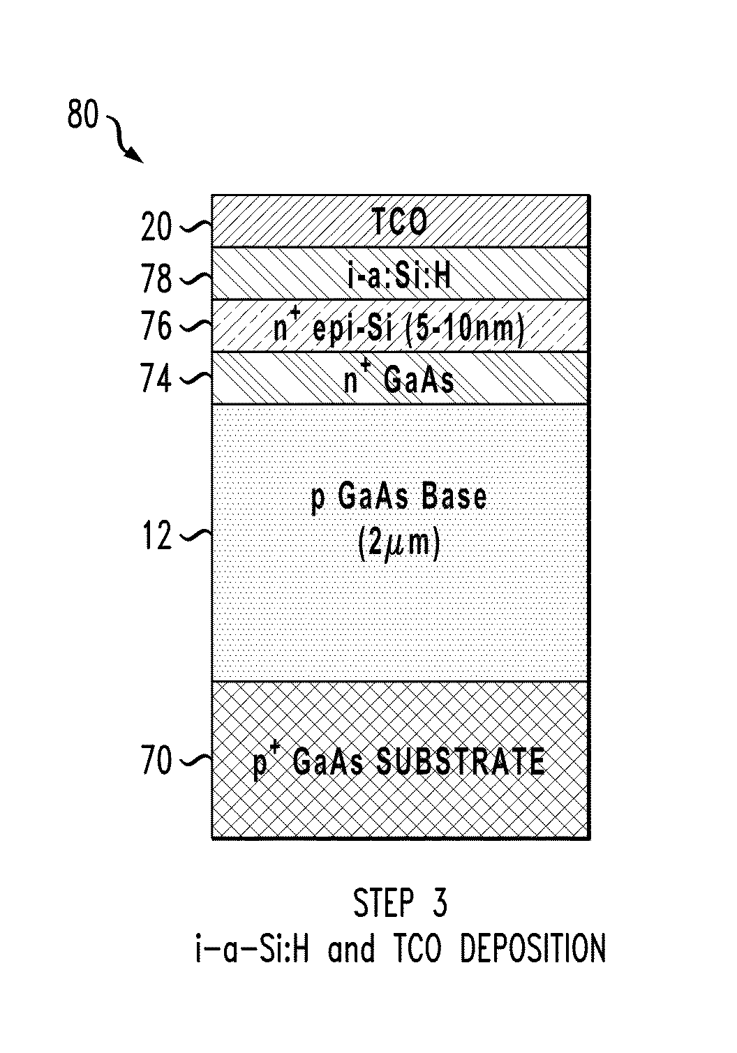
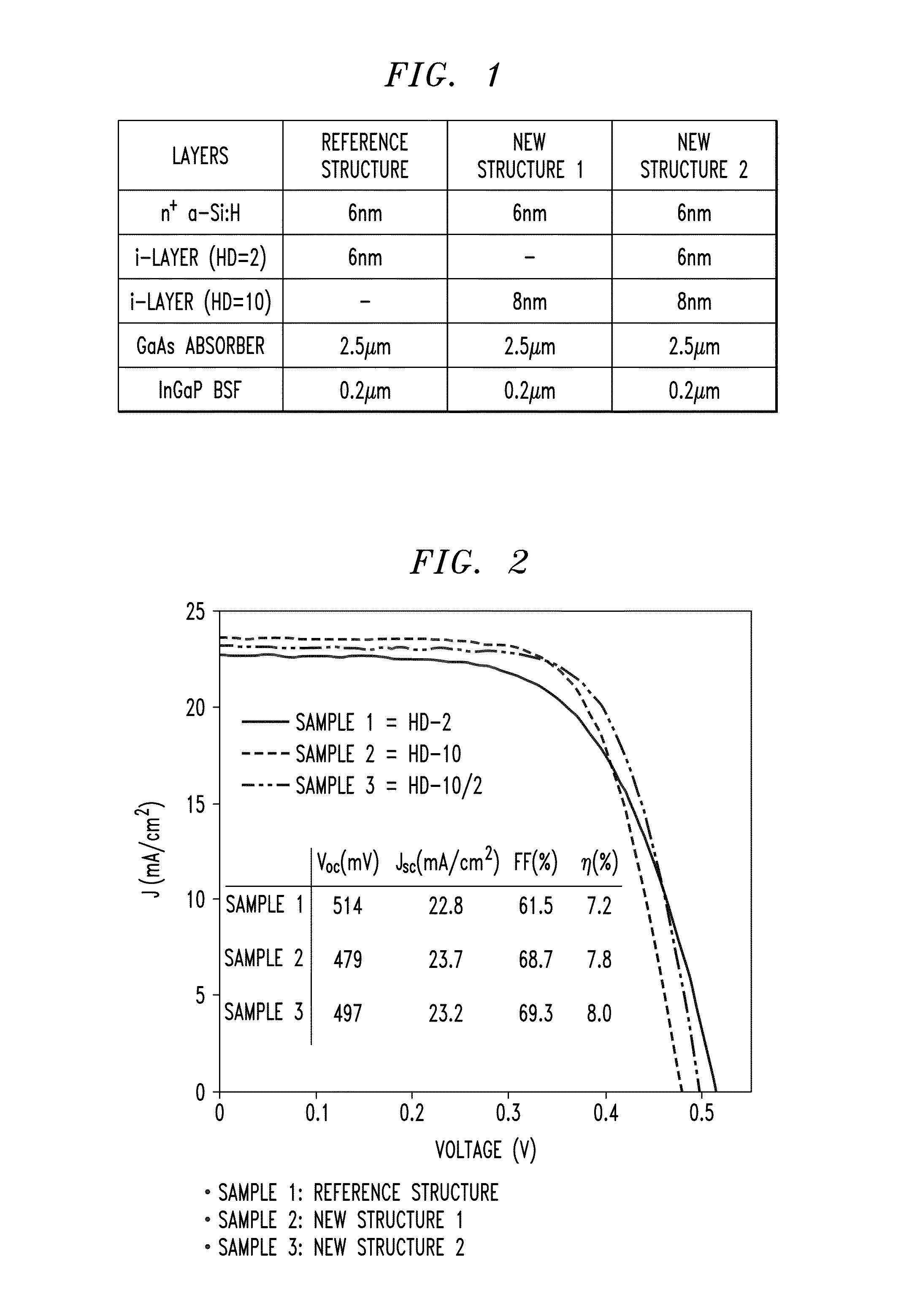
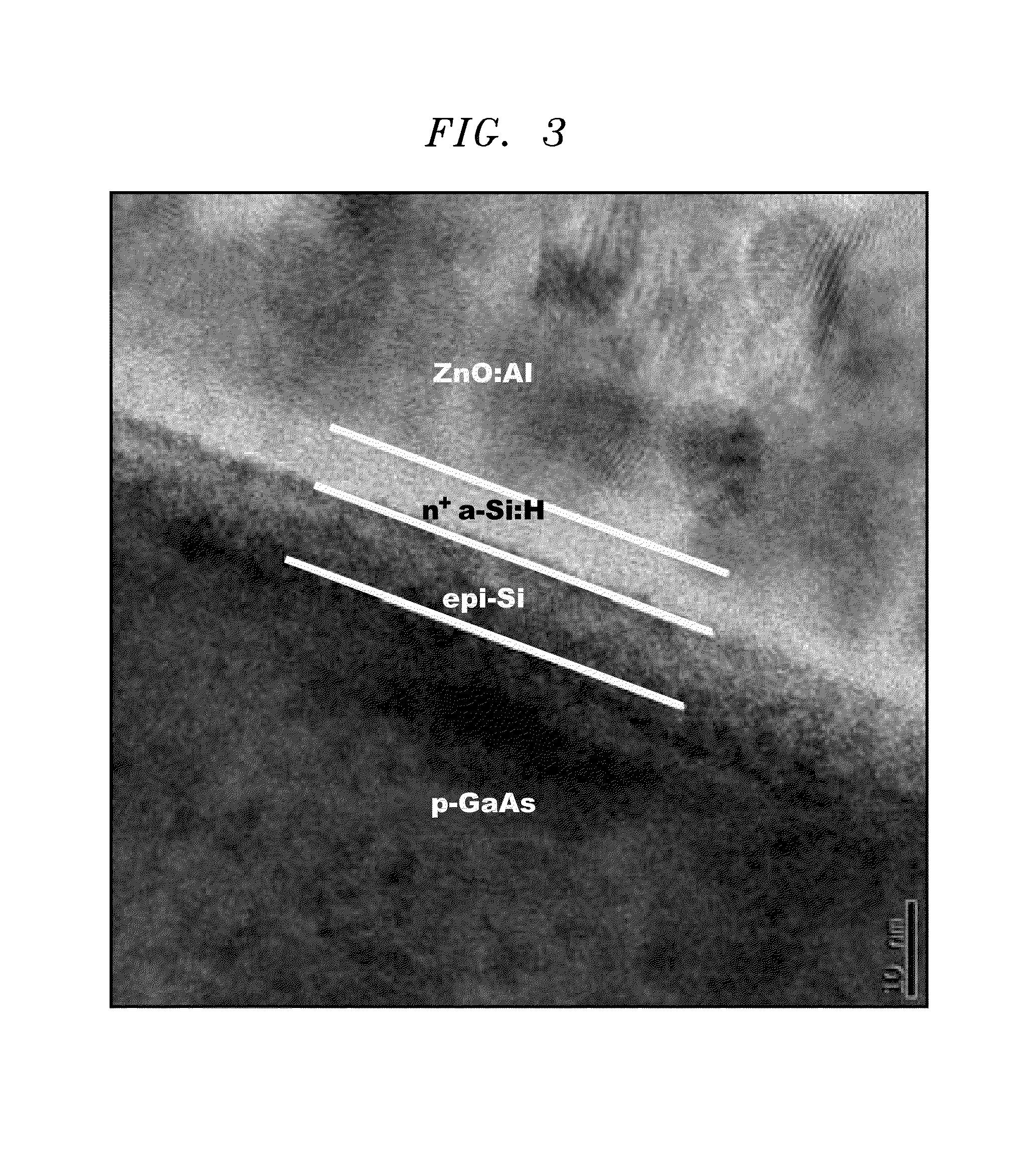
[0022]Heterojunction III-V solar cell structures based on a-Si:H / III-V heterostructures offer a path for low-cost, high efficiency PV (photovoltaic) technology when implemented in conjunction with a layer transfer technique. The use of a-Si:H as an intrinsic layer (i-a:Si:H) can significantly improve the surface passivation of GaAs. US Pub. No. 2010 / 0307572 entitled “Heterojunction III-V Photovoltaic Cell Fabrication”, the disclosure of which is incorporated by reference herein, discloses techniques for forming single and double heterojunction III-V PV cells.

[0023]FIG. 4 shows a solar cell structure 10 that can be produced using techniques disclosed in US Pub. No. 2010 / 0307572. The structure 10 includes a base layer 12 comprising a doped III-V substrate that may be n-type or p-type. Doped amorphous silicon layers 18, 18′ are formed on intrinsic amorphous silicon layers 16 on the base layer 12. The amorphous silicon layers 18, 18′ may have doping types that are the same or opposite f...


PUM


Abstract

Solar cell structures that have improved carrier collection efficiencies at a heterointerface are provided by low temperature epitaxial growth of silicon on a III-V base. Additionally, a solar cell structure having improved open circuit voltage includes a shallow junction III-V emitter formed by epitaxy or diffusion followed by the epitaxy of SixGe1-x passivated by amorphous SiyGe1-y:H.

Description

FIELD OF THE INVENTION[0001]The present invention relates to the physical sciences, and, more particularly, to solar cell structures comprising III-V absorber materials.BACKGROUND OF THE INVENTION[0002]Direct gap III-V materials such as gallium arsenide are attractive candidates for making high efficiency solar cells due to their strong absorption properties. The fabrication of high efficiency III-V solar cells can be achieved by epitaxial growth of the structures using various techniques such as metalorganic chemical vapor deposition and molecular beam epitaxy, the cost of which renders them relatively expensive for many terrestrial applications. Alternative approaches have been proposed such as formation of ITO Schottky contacts and zinc diffusion. Such approaches do not, however, provide a platform for manufacturing high efficiency cells due to the lack of proper surface passivation.SUMMARY OF THE INVENTION[0003]Principles of the invention provide techniques for improving solar c...

Claims


Application Information

Patent Timeline
Patent Type & Authority Patents(United States)
IPC IPC(8): H01L31/18H01L31/20
CPCY02E10/50H01L31/20H01L31/036H01L31/077H01L31/0304Y02E10/544Y02E10/547Y02E10/548Y02P70/50H01L31/02167H01L31/022466H01L31/074
Inventor BEDELL, STEPHEN W.HEKMATSHOARTABARI, BAHMANSADANA, DEVENDRA K.SHAHRJERDI, DAVOOD
Owner IBM CORP
Why Eureka
Try Eureka