Organic electroluminescent device and preparation method thereof
an electroluminescent device and organic technology, applied in the direction of electroluminescent light sources, thermoelectric devices, electric lighting sources, etc., can solve the problems of holes, deterioration of device characteristics and lifetime, and difficult to find an example of introducing inorganic matter layers into the inside of light-emitting layers
- Summary
- Abstract
- Description
- Claims
- Application Information
AI Technical Summary
Benefits of technology
Problems solved by technology
Method used
Image
Examples
example 1
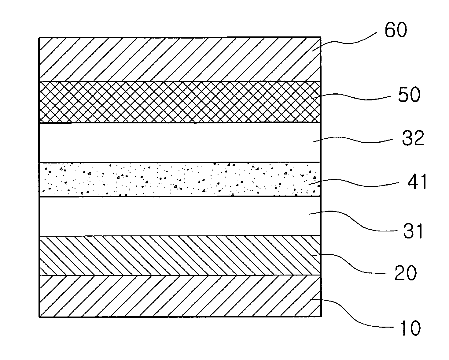
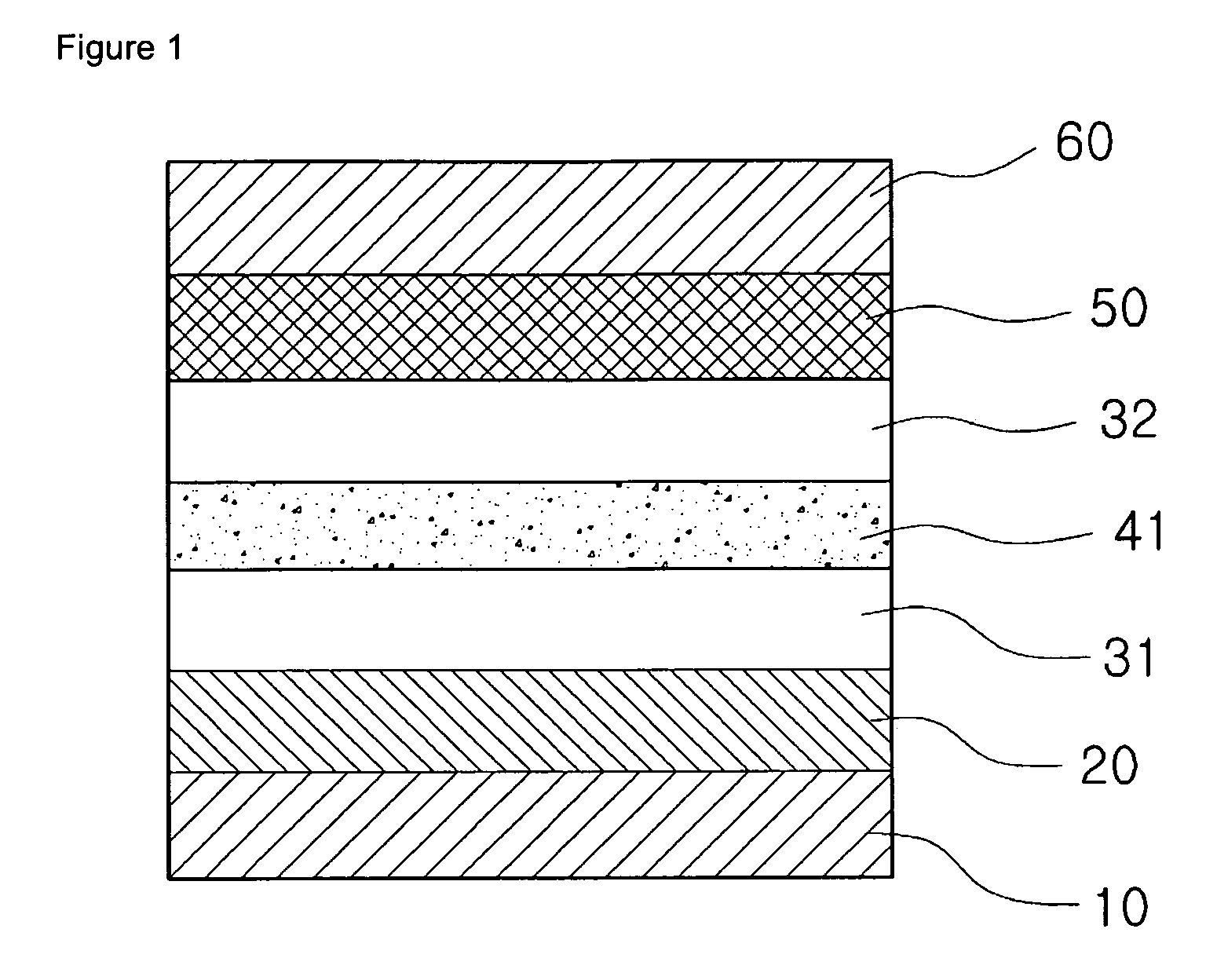
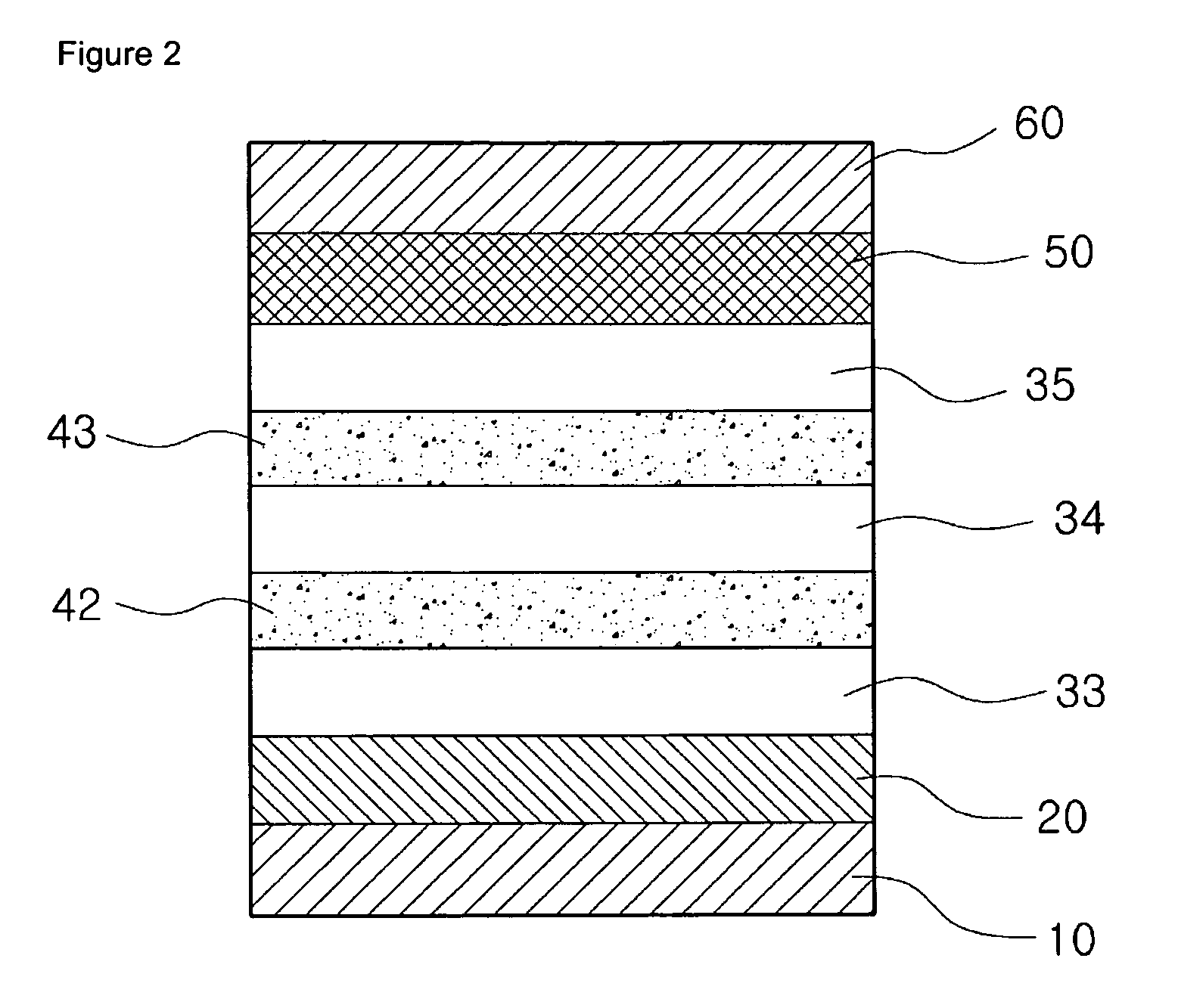
[0035]A 15 Ω / cm2 (120 nm) ITO glass substrate as an anode electrode is cut at a proper size and is cleaned in isopropyl alcohol and pure water by means of ultrasonic wave for 10 minutes and is cleaned by means of UV or ozone for 20 minutes. A PEDOT / PSS (product available from Bayer Co.; Poly(3,4-ethylenedioxythiophene) / Poly(styrene sulfonic acid)) aqueous solution is spin-coated on the upper of the substrate to form a hole injection layer of 40 nm in thickness. Then, a light-emitting layer of 40 nm in thickness is formed on the hole injection layer by spin-coating the mixture of the 95:5 weight percent of PVK (Poly(9-vinylcarbazole) available form Aldrich Co.) and Flrpic (Iridium(III) bis[(4,6-difluorophenyl)pyridinato-N,C2′]picolinate), which is blue phosphor light-emitting material, and a zirconium oxide intermediate layer of 10 nm in thickness is then formed on the upper of the light-emitting layer by spin-coating zirconium oxide solution dissolved with D40 (product form EXXON Co...
example 2
[0036]A 15 Ω / cm2 (120 nm) ITO glass substrate as an anode electrode is cut at a proper size and is cleaned in isopropyl alcohol and pure water by means of ultrasonic wave for 10 minutes and is cleaned by means of UV or ozone for 20 minutes. A PEDOT / PSS (hole injection material which is product from Bayer Co.) aqueous solution is spin-coated on the upper of the substrate to form a hole injection layer of 40 nm in thickness. Then, a light-emitting layer of 40 nm in thickness is formed on the hole injection layer by spin-coating the mixture of the 95:5 weight percent of PVK and Ir(ppy)3 (fac-tris(2-phenylpyridinato)iridium), which is green phosphor light-emitting material, and a zirconium oxide intermediate layer of 10 nm in thickness is then formed on the upper of the light-emitting layer by spin-coating zirconium oxide solution dissolved with D40 (product form EXXON Co.) solvent. Thereafter, the light-emitting layer of 40 nm in thickness is formed on the zirconium oxide intermediate ...
example 3
[0037]A 15 Ω / cm2 (120 nm) ITO glass substrate as an anode electrode is cut at a proper size and is cleaned in isopropyl alcohol and pure water by means of ultrasonic wave for 10 minutes and is cleaned by means of UV or ozone for 20 minutes. A PEDOT / PSS aqueous solution is spin-coated on the upper of the substrate to form a hole injection layer of 40 nm in thickness. Then, a light-emitting layer of 40 nm in thickness is formed on the hole injection layer by spin-coating the mixture of the 95:5 weight percent of PVK and Btp2Ir(acac)(Iridium(III) bis(2-(2′-benzothienyl)pyridinato-N,C3′)(acetylacetonate), which is red phosphor light-emitting material, and a zirconium oxide intermediate layer of 10 nm in thickness is then formed on the upper of the light-emitting layer by spin-coating zirconium oxide solution dissolved with D40 (product form EXXON Co.) solvent. Thereafter, the light-emitting layer of 40 nm in thickness is formed on the zirconium oxide intermediate layer by spin-coating t...
PUM
 Abstract
Description
Claims
Application Information
 - R&D
- Intellectual Property
- Life Sciences
- Materials
- Tech Scout
- Unparalleled Data Quality
- Higher Quality Content
- 60% Fewer Hallucinations
Browse by: Latest US Patents, China's latest patents, Technical Efficacy Thesaurus, Application Domain, Technology Topic, Popular Technical Reports.
© 2025 PatSnap. All rights reserved.Legal|Privacy policy|Modern Slavery Act Transparency Statement|Sitemap|About US| Contact US: help@patsnap.com


