
Apparatus and method for processing substrate

a substrate and apparatus technology, applied in the field of apparatus and method for processing substrates, can solve the problems of bending substrates, large installation space, and difficulty in aligning substrates, and achieve the effects of less contamination, less contamination, and improved space utility of production lines

Active Publication Date: 2014-10-21
CHARM ENG CO LTD
View PDF15 Cites 1 Cited by
  • Summary
  • Abstract
  • Description
  • Claims
  • Application Information

AI Technical Summary

Benefits of technology

The patent describes an apparatus for processing a substrate that allows for individual plasma processing on each edge and rear region of the substrate in a single chamber. This means that the edge region of the substrate is protected while it is processed, while the rear region is protected while it is processed. This reduces the space needed for the apparatus and improves the space utilization of production lines. Additionally, there is no exposure of the substrate to the atmosphere, reducing contamination, and there is no standby time, resulting in a reduction of the overall processing time.

Problems solved by technology

Meanwhile, in a thin film deposition process, a thin film may be deposited not only in a desired central region of a substrate but also in undesired edge and rear regions of the substrate.
If subsequent processes are continuously performed in a state where the thin film and particles accumulated on the substrate are not removed, there may be many problems in that the substrate is bent or the alignment of the substrate may be difficult.
However, since conventional edge and rear etching devices separately exist as independent devices, a broad installation space has been required.
Therefore, it is highly likely that the substrate subjected to processing is exposed to the atmosphere and contaminated.

Method used


Image

  • Apparatus and method for processing substrate
  • Apparatus and method for processing substrate
  • Apparatus and method for processing substrate

Examples


first embodiment

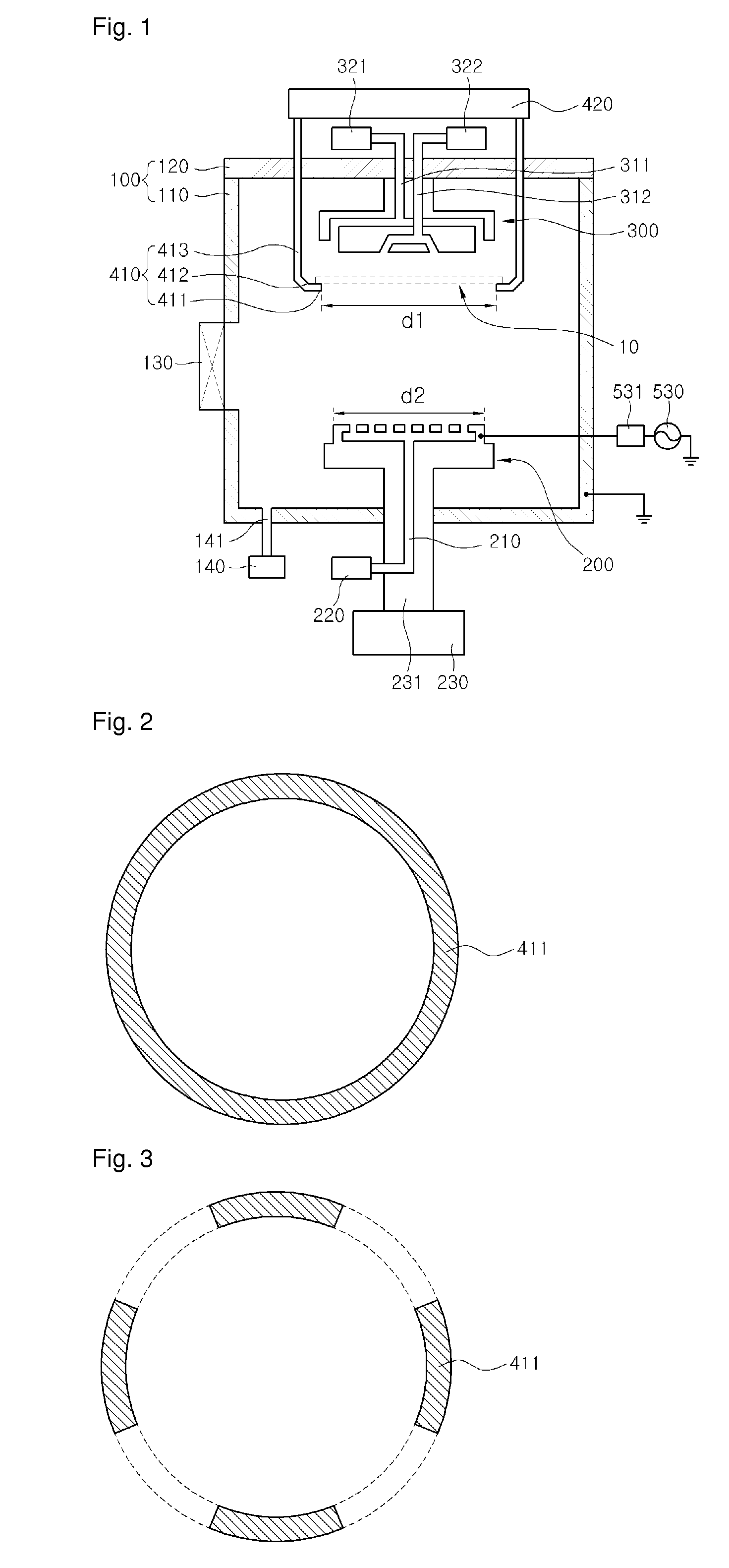
[0034]FIG. 1 is a schematic view showing an apparatus for processing a substrate according to a first embodiment of the present invention, and FIGS. 2 and 3 are bottom surfaces of support portions of a support according to the first embodiment of the present invention.

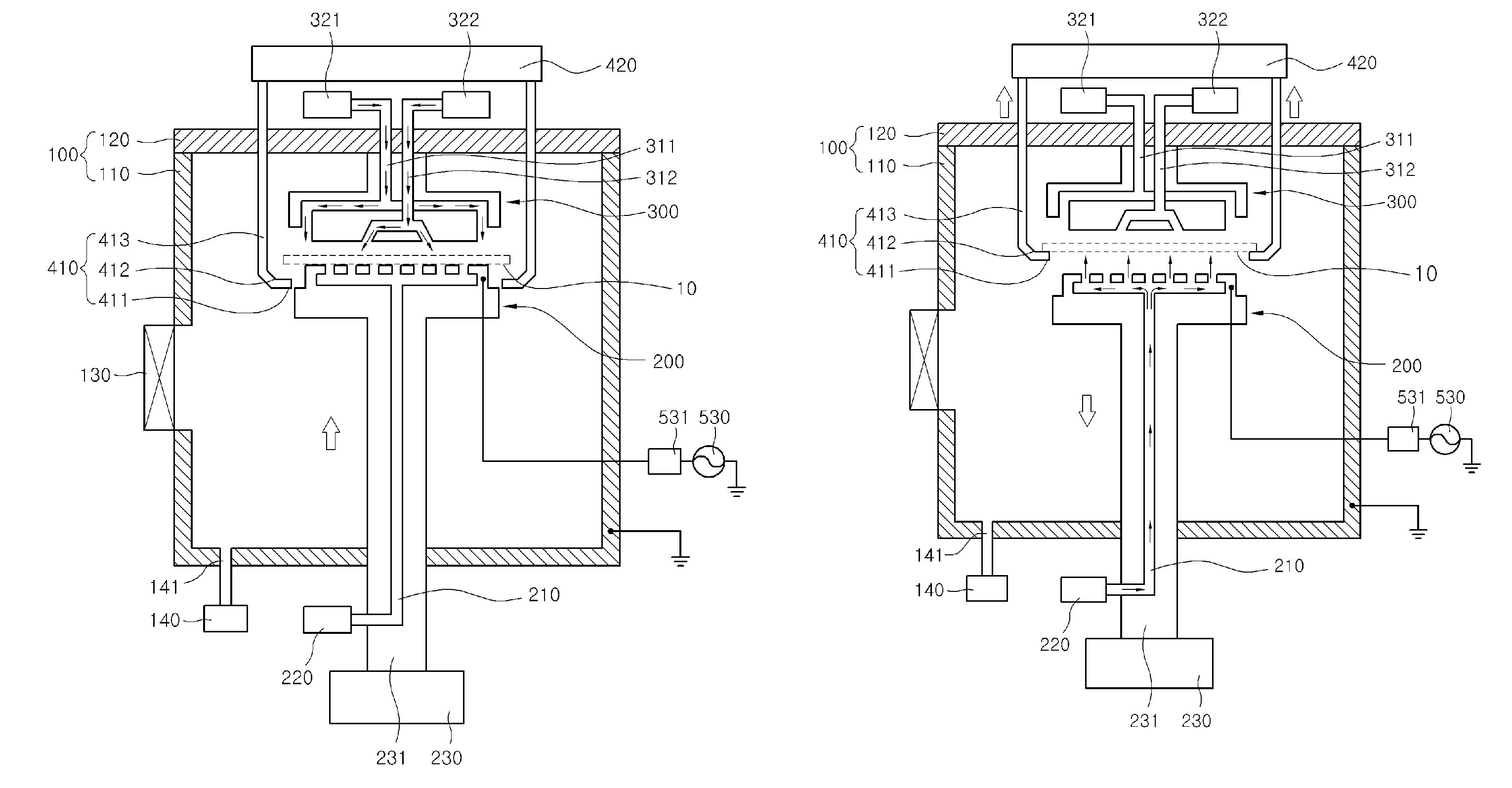
[0035]Referring to FIG. 1, the apparatus for processing a substrate according to this embodiment includes: a chamber 100 having a reaction space provided therein; a stage 200 installed at a lower part of the interior of the chamber 100; a plasma shielding unit 300 installed at an upper part of the interior of the chamber 100 opposite to the stage 200; a support unit 410 configured to support a substrate between the stage 200 and the plasma shielding unit 300; and a plasma generating unit 510, 520 and 530 for generating plasma between the stage 200 and the plasma shielding unit 300. Here, the substrate 10 refers to a plate-shaped object to be processed, e.g., a wafer, a glass panel or the like, which is required to be p...

second embodiment

[0049]The aforementioned apparatus for processing a substrate is not limited to the aforementioned configuration but may variously be modified. Hereinafter, an apparatus for processing a substrate according to a second embodiment of the present invention will be described as an example of the modifications. At this time, descriptions overlapping with the aforementioned embodiment will be omitted or briefly described.

[0050]FIG. 7 is a schematic view of an apparatus for processing a substrate according to the second embodiment of the present invention.

[0051]Referring to FIG. 7, the apparatus for processing a substrate according to this embodiment includes a chamber 100 having a reaction space provided therein; a stage 200 installed at a lower part of the interior of the chamber 100; a plasma shielding unit 600 installed at an upper part of the interior of the chamber 100 opposite to the stage 200; a support unit 710 allowing a substrate to be supported between the stage 200 and the pl...


PUM

PropertyMeasurementUnit
distanceaaaaaaaaaa
widthaaaaaaaaaa
areaaaaaaaaaaa

Abstract

There are provided an apparatus and method for processing a substrate. By using the apparatus and method, plasma processing can be individually performed on each of edge and rear regions of a substrate in a single chamber. The apparatus includes a chamber providing a reaction space; a stage installed in the chamber; a plasma shielding unit installed opposite to the stage in the chamber; a support unit for supporting a substrate between the stage and the plasma shielding unit; a first supply pipe provided at the stage to supply a reaction or non-reaction gas to one surface of the substrate; and second and third supply pipes provided at the plasma shielding unit, the second supply pipe supplying a reaction gas to the other surface of the substrate, the third supply pipe supplying a non-reaction gas to the other surface.

Description

TECHNICAL FIELD[0001]The present invention relates to an apparatus and method for processing a substrate, and more particularly, to an apparatus and method for processing a substrate, wherein plasma processing can be individually performed on each of edge and rear regions of a substrate in a single chamber.BACKGROUND ART[0002]A semiconductor device is fabricated by performing thin film deposition and etching processes. That is, a thin film is formed in a predetermined region on a substrate by performing a deposition process, and an unnecessary portion of the thin film is removed by performing an etching process using an etching mask, thereby forming a desired circuit pattern or circuit element on the substrate to fabricate a semiconductor device. Generally, such deposition and etching processes are repeated several times until a desired circuit pattern is obtained.[0003]Meanwhile, in a thin film deposition process, a thin film may be deposited not only in a desired central region of...

Claims


Application Information

Patent Timeline
Patent Type & Authority Patents(United States)
IPC IPC(8): H01J37/20C23C16/00H01L21/306C23F1/00H01J37/32
CPCH01J37/3244H01J37/32449H01J37/20H01J2237/20235H01J2237/2002H01L21/67069H01L21/68785H01L21/68742H01J37/32715H01J37/32385
Inventor HAN, YOUNG KISEO, YOUNG SOO
Owner CHARM ENG CO LTD
Learn More