
Silane and borane treatments for titanium carbide films

a titanium carbide and treatment technology, applied in the direction of semiconductor/solid-state device manufacturing, basic electric elements, electric devices, etc., can solve the problems of limiting the maximum deposition temperature, limiting the growth temperature, and still having problems with impurity content in ald films, so as to reduce the oxidized portions

Active Publication Date: 2014-09-23
ASM IP HLDG BV
View PDF191 Cites 390 Cited by
  • Summary
  • Abstract
  • Description
  • Claims
  • Application Information

AI Technical Summary

Benefits of technology

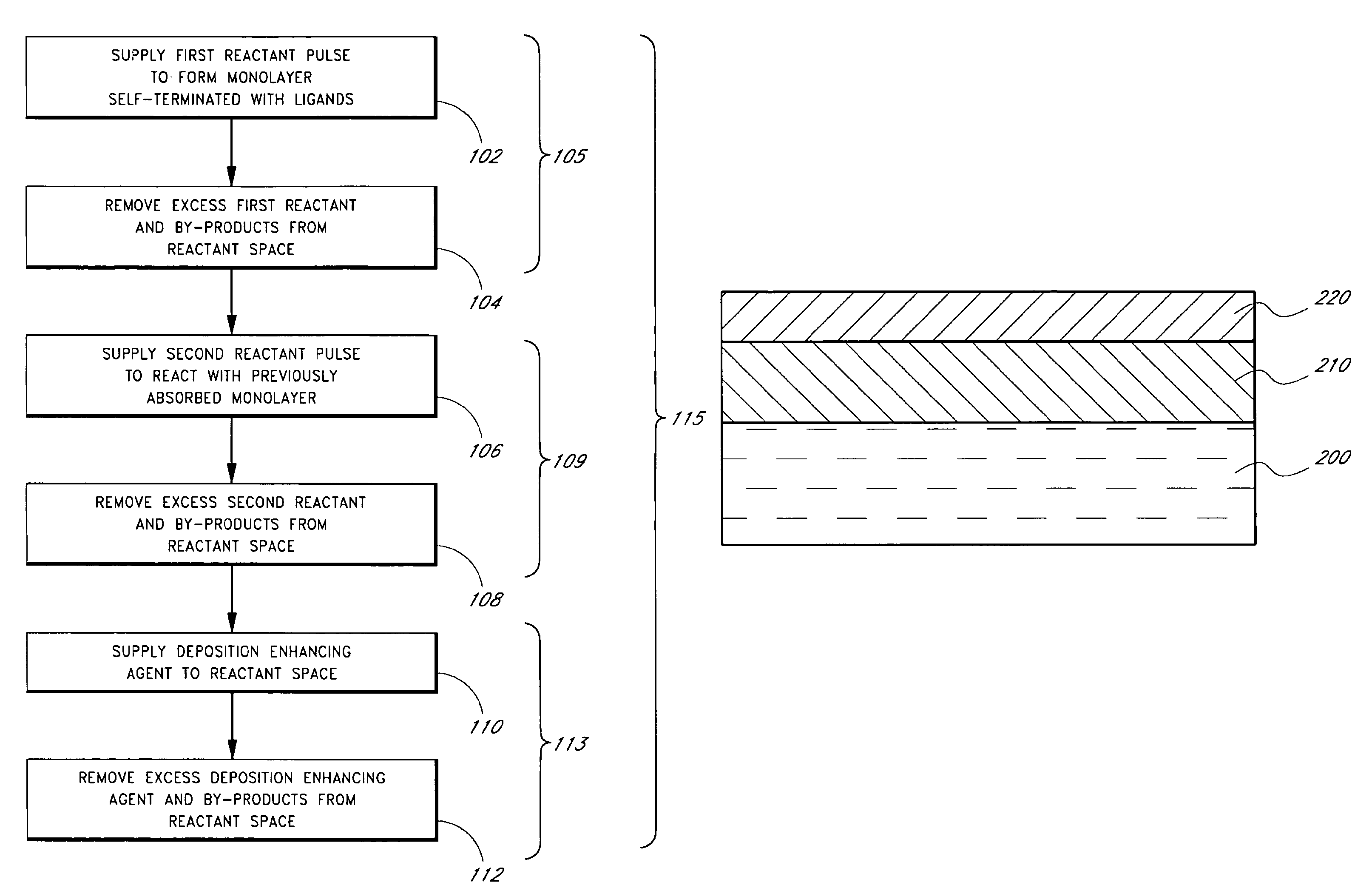
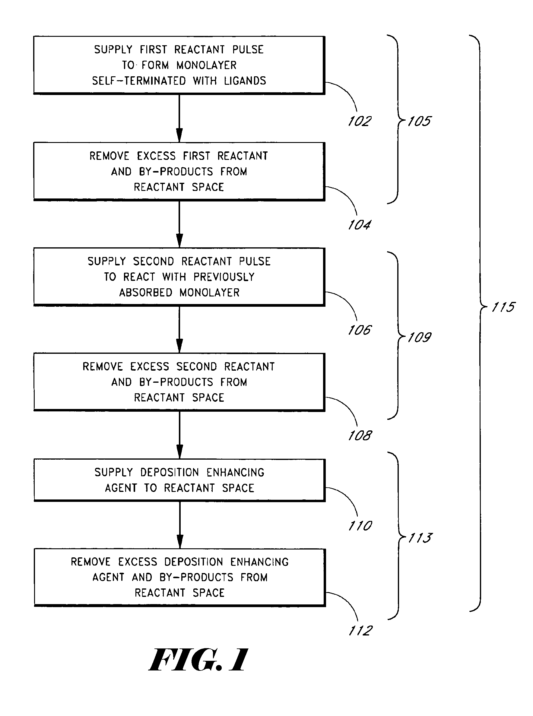
[0008]According to some embodiments of the invention, an organosilane, organoborane, silane, or borane (generally referred to herein as a “silane / borane agent”) is utilized in atomic layer deposition (ALD) processes for depositing a boron- or silicon-containing film comprising metal carbide from a halide-containing precursor or in treating a deposited film that comprises metal carbide. The silane / borane agent may be pulsed during or after a deposition cycle, or it may be applied to a thin film after some or all cycles have been completed. In some embodiments, the silane / borane agent may serve to reduce oxidized portions of a metal film. In some embodiments, the silane / borane agent may form a barrier to at least partially prevent further oxidation of the film itself or of films subsequently deposited over the treated film. In some embodiments, the silane / borane agent may help in gettering oxygen from deeper within a film, such as oxygen coming from subsequent air exposure.
[0010]In some cases, the barrier effect of the silane / borane agent treatment may also prevent or limit oxidation of one or more layers deposited after the silane / borane treatment of the metal carbide film. For example, the use of a silane / borane agent in the formation or treatment of a metal carbide film, such as a titanium carbide film, may limit oxidation of a second film deposited over the titanium carbide film, such as a nitride film (for example TiN) even if the second film is not itself treated with a silane / borane agent. Additional subsequently deposited films may also be protected from oxidation by the silane / borane agent treatment of the metal carbide layer.

Problems solved by technology

Despite the lower impurity levels in ALD films, the impurity content in ALD films can still be a problem.
In some cases, the semiconductor process flow necessarily limits the maximum deposition temperature such that that some residues are left in the film.
Halide impurities are present mainly at the interfaces, which can also lead to problems.
In another example, in some applications amorphous films are needed, which limits the growth temperature.

Method used


Image

  • Silane and borane treatments for titanium carbide films
  • Silane and borane treatments for titanium carbide films
  • Silane and borane treatments for titanium carbide films

Examples


example 1

TiC Films

[0112]Using the methods disclosed here in, various titanium carbide thin films were deposited. The thin film was then analyzed using Rutherford backscattering spectrometry, or RBS, to determine the composition of the various films.

[0113]After analyzing the various films, it was determined that they the following ranges of compositions on an atomic basis: about 17-20% Ti, about 17-27% Al, about 16-42% Si, and about 21-39% C.

example 2

TiAlC and TiAlSiC in a Single Wafer Reactor

[0114]Titanium-aluminium carbide (TiAlC) and titanium-aluminum-carbide-silicon (TiAlSiC) thin films were deposited by Atomic layer deposition (ALD) in Pulsar® 2000 R&D reactor using TiCl4 as the titanium source and Al(CH2CH3)3 as the aluminum and carbon source for the TiAlC films and in addition disilane (Si2H6) or trisilane (Si3H8) was used as a silicon source for TiAlSiC films.

[0115]TiAlC and TiAlSiC films were deposited using alternate and sequential pulses of TiCl4 and Al(CH2CH3)3 and in the case of TiAlSiC films additional alternate and sequential pulses of disilane (Si2H6) or trisilane (Si3H8) were provided. TiAlC films were also soaked with disilane (Si2H6) or trisilane (Si3H8) for about 1 minute. Films were deposited and treated at a reaction temperature of about 415° C. TiCl4 was pulsed for 0.05 s and purged for 5 s. Al(CH2CH3)3 was pulsed for 0.5 s and purged for 5 s. Si2H6 or Si3H8 was pulsed for 0.5 s and purged for 5 s. The Al(...


PUM

PropertyMeasurementUnit
thicknessaaaaaaaaaa
workfunctionaaaaaaaaaa
thickaaaaaaaaaa

Abstract

Methods of treating metal-containing thin films, such as films comprising titanium carbide, with a silane / borane agent are provided. In some embodiments a film including titanium carbide is deposited on a substrate by an atomic layer deposition (ALD) process. The process may include a plurality of deposition cycles involving alternating and sequential pulses of a first source chemical that includes titanium and at least one halide ligand, a second source chemical that includes metal and carbon, where the metal and the carbon from the second source chemical are incorporated into the thin film, and a third source chemical, where the third source chemical is a silane or borane that at least partially reduces oxidized portions of the titanium carbide layer formed by the first and second source chemicals. The treatment can form a capping layer on the metal carbide film.

Description

BACKGROUND OF THE INVENTION[0001]1. Field of the Invention[0002]The present invention relates generally to processes for producing metal carbide thin films on a substrate by atomic layer deposition. In some embodiments, titanium carbide films produced by the atomic layer deposition (ALD) processes disclosed herein can be used in metal gate and metal electrode applications in metal oxide semiconductor field effect transistors (MOSFETs), such as n-channel MOSFETs (NMOS).[0003]2. Description of the Related Art[0004]Atomic layer deposition (ALD) is a generally self-limiting process, whereby alternated pulses of reaction precursors saturate a substrate surface and leave no more than about one monolayer of material per pulse. The deposition conditions and precursors are selected to provide self-saturating reactions, such that an adsorbed layer in one pulse leaves a surface termination that is non-reactive with the gas phase reactants of the same pulse. A subsequent pulse of different reac...

Claims


Application Information

Patent Timeline
Patent Type & Authority Patents(United States)
IPC IPC(8): H01L21/336H01L21/8234H01L21/02
CPCH01L21/02186H01L21/022H01L21/02337H01L21/02321H01L21/0228H01L21/28044H01L21/2807H01L21/28088H01L21/28556H01L21/28568
Inventor CHEN, JERRYMACHKAOUTSAN, VLADIMIRMILLIGAN, BRENNANMAES, JAN WILLEMHAUKKA, SUVISHERO, ERICBLOMBERG, TOM E.LI, DONG
Owner ASM IP HLDG BV
Learn More