Photoelectric conversion element
a technology of conversion element and photoelectric, applied in the direction of basic electric elements, electrical equipment, semiconductor devices, etc., can solve the problems of reducing light absorption, achieve the effect of improving light absorption efficiency, increasing manufacturing cost, and improving photoelectric conversion efficiency
- Summary
- Abstract
- Description
- Claims
- Application Information
AI Technical Summary
Benefits of technology
Problems solved by technology
Method used
Image
Examples
embodiment 1
[Embodiment 1]
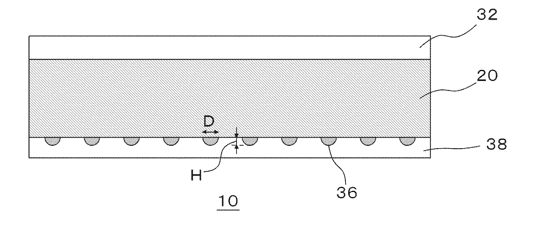
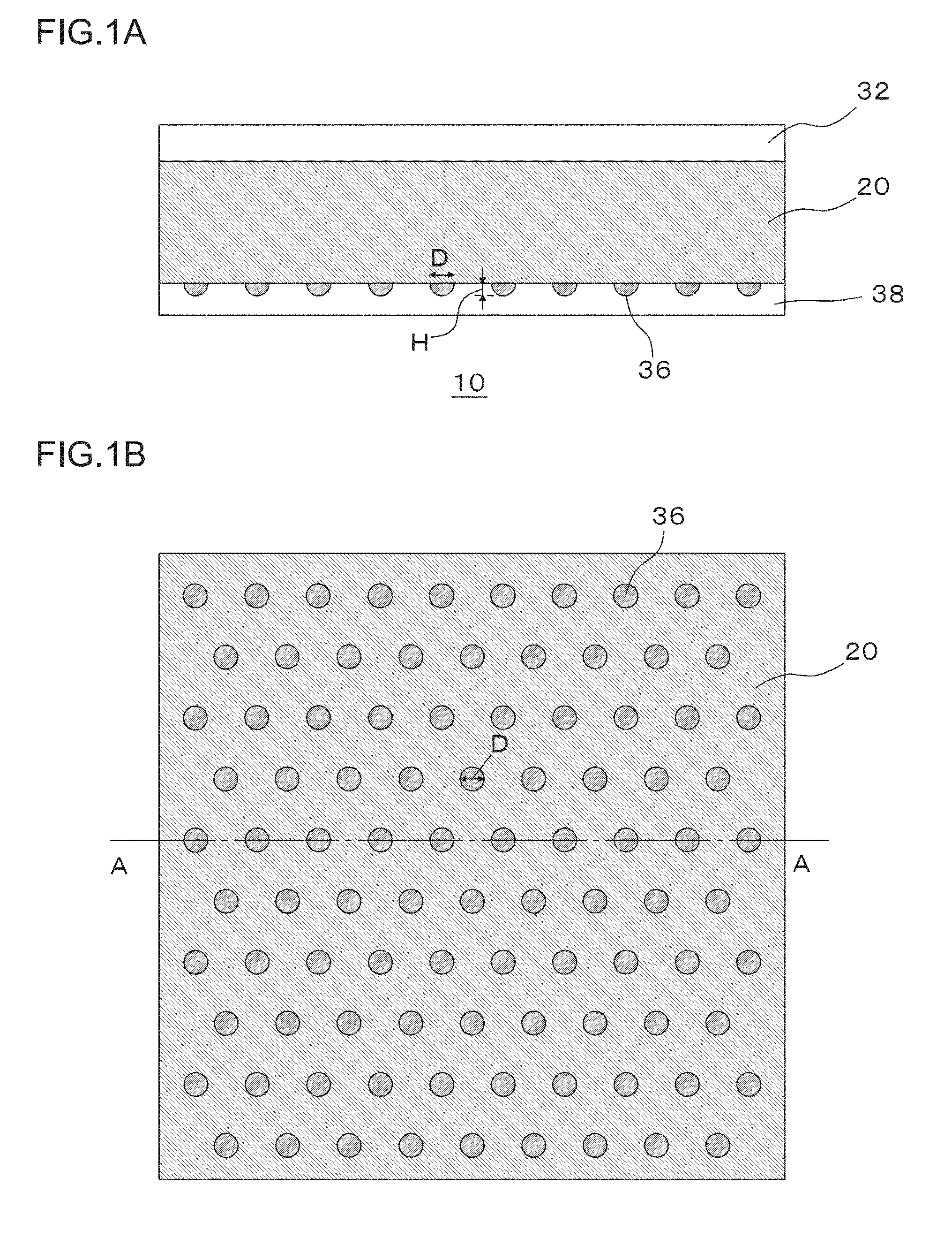
[0041]FIG. 1A is a schematic cross-sectional view showing a structure of a photoelectric conversion element according to an embodiment 1. FIG. 1B is a plan view showing a metal nanoparticle array included in the photoelectric conversion element as viewed from the side that is opposite to the light receiving face.
[0042]FIG. 1A corresponds to a cross-sectional view taken along line A-A in FIG. 1B. In FIG. 1B, a dielectric layer 38 is not shown.
[0043]As shown in FIG. 1A, a photoelectric conversion element 10 includes a photoelectric conversion layer 20, an antireflection film 32, multiple metal nanoparticles 36, and a dielectric layer 38. With the present embodiment, the photoelectric conversion element 10 is configured as a solar cell.
[0044]The photoelectric conversion layer 20 has a pn junction obtained by combining a P-type semiconductor and an N-type semiconductor, which allows solar light energy to be converted into electric energy by means of the photovoltaic effect...
embodiment 2
[Embodiment 2]
[0060]FIG. 3 is a schematic cross-sectional diagram showing a configuration of a photoelectric conversion element 10 according to an embodiment 2. With the photoelectric conversion element 10 according to the present embodiment, each metal nanoparticle 36 is not directly in contact with the second principal face of the photoelectric conversion layer 20. Instead, a transparent thin film 50 is formed between each metal nanoparticle 36 and the second principal face of the photoelectric conversion layer 20. The transparent thin film 50 is configured to be transparent to the light to be received by the photoelectric conversion element 10. That is to say, the transparent thin film 50 has a bandgap that is greater than that of the photoelectric conversion layer 20. Furthermore, in a case in which an electrode is formed on the second principal face side of the photoelectric conversion layer 20, from the viewpoint of improving the current collecting efficiency, the transparent ...
example 1-1
[Production of Photoelectric Conversion Layer]
[0063]An a-SiOx:H layer having a thickness of 5 nm was laminated as an i-layer on one face of a p-type silicon wafer (having resistivity of 0.5 to 5 Ωcm) having a thickness of 100 μm. Furthermore, an n-type a-Si:H layer having a thickness of 7.5 nm was laminated on the i-layer, thereby forming a photoelectric conversion layer. The results of using a spectroscopic ellipsometer to measure the refractive index of the p-type silicon wafer indicated a refractive index of 3.9 at a wavelength of 600 nm.
[Production of Antireflection Film]
[0064]An ITO film having a thickness of 75 nm was formed as an antireflection film on the n-type a-Si:H layer.
[Production of Transparent Thin Film Layer]
[0065]A p-type microcrystalline SiOx:H having a thickness of 30 nm was formed as a transparent thin film layer on the exposed face (back face) of the p-type silicon wafer. The results of using X-ray photoelectron spectroscopy to measure the oxygen content of the...
PUM
| Property | Measurement | Unit |
|---|---|---|
| refractive index | aaaaa | aaaaa |
| diameter | aaaaa | aaaaa |
| diameter | aaaaa | aaaaa |
Abstract
Description
Claims
Application Information
 - Generate Ideas
- Intellectual Property
- Life Sciences
- Materials
- Tech Scout
- Unparalleled Data Quality
- Higher Quality Content
- 60% Fewer Hallucinations
Browse by: Latest US Patents, China's latest patents, Technical Efficacy Thesaurus, Application Domain, Technology Topic, Popular Technical Reports.
© 2025 PatSnap. All rights reserved.Legal|Privacy policy|Modern Slavery Act Transparency Statement|Sitemap|About US| Contact US: help@patsnap.com


