
Method of fabricating semiconductor structure

a technology of semiconductor structure and fabrication method, which is applied in the direction of semiconductor/solid-state device details, diodes, radio frequency controlled devices, etc., can solve the problems of low throughput, low throughput, and high complexity of the sensor fabrication process, so as to improve the light absorption efficiency of the cmos sensor, the effect of reducing costs and improving throughpu

Active Publication Date: 2015-12-03
OMNIVISION TECH (SHANGHAI) CO LTD
View PDF0 Cites 0 Cited by
  • Summary
  • Abstract
  • Description
  • Claims
  • Application Information

AI Technical Summary

Benefits of technology

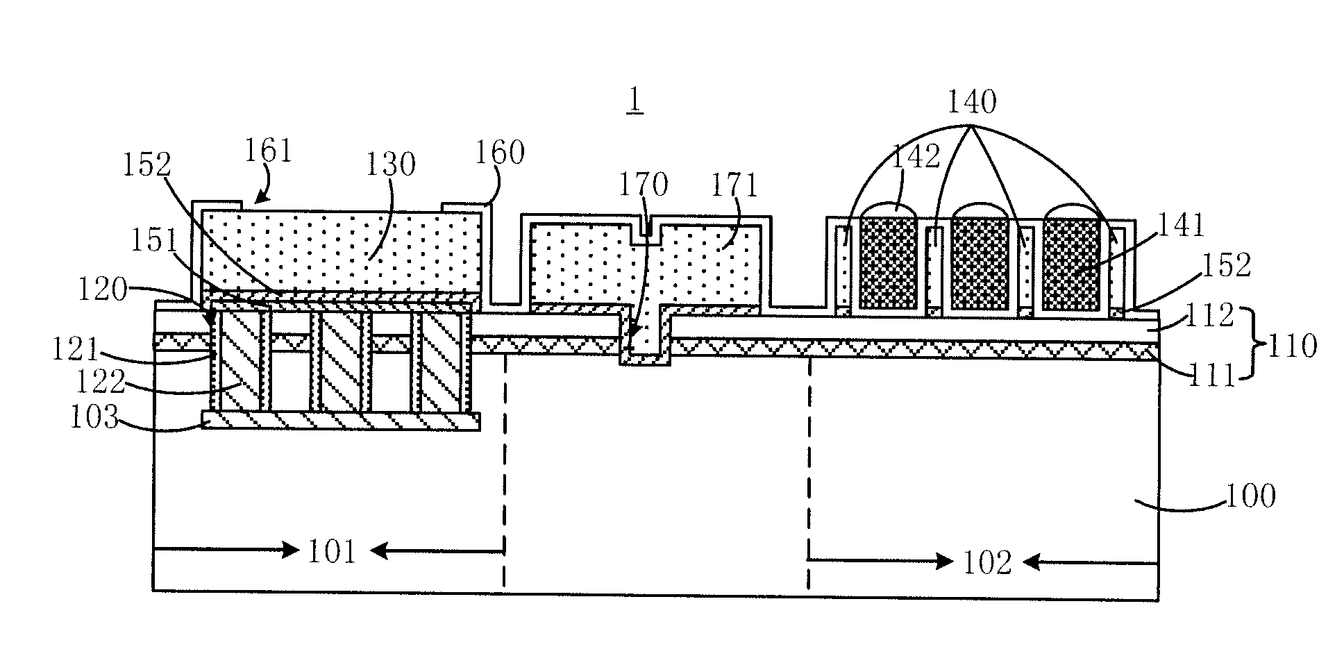
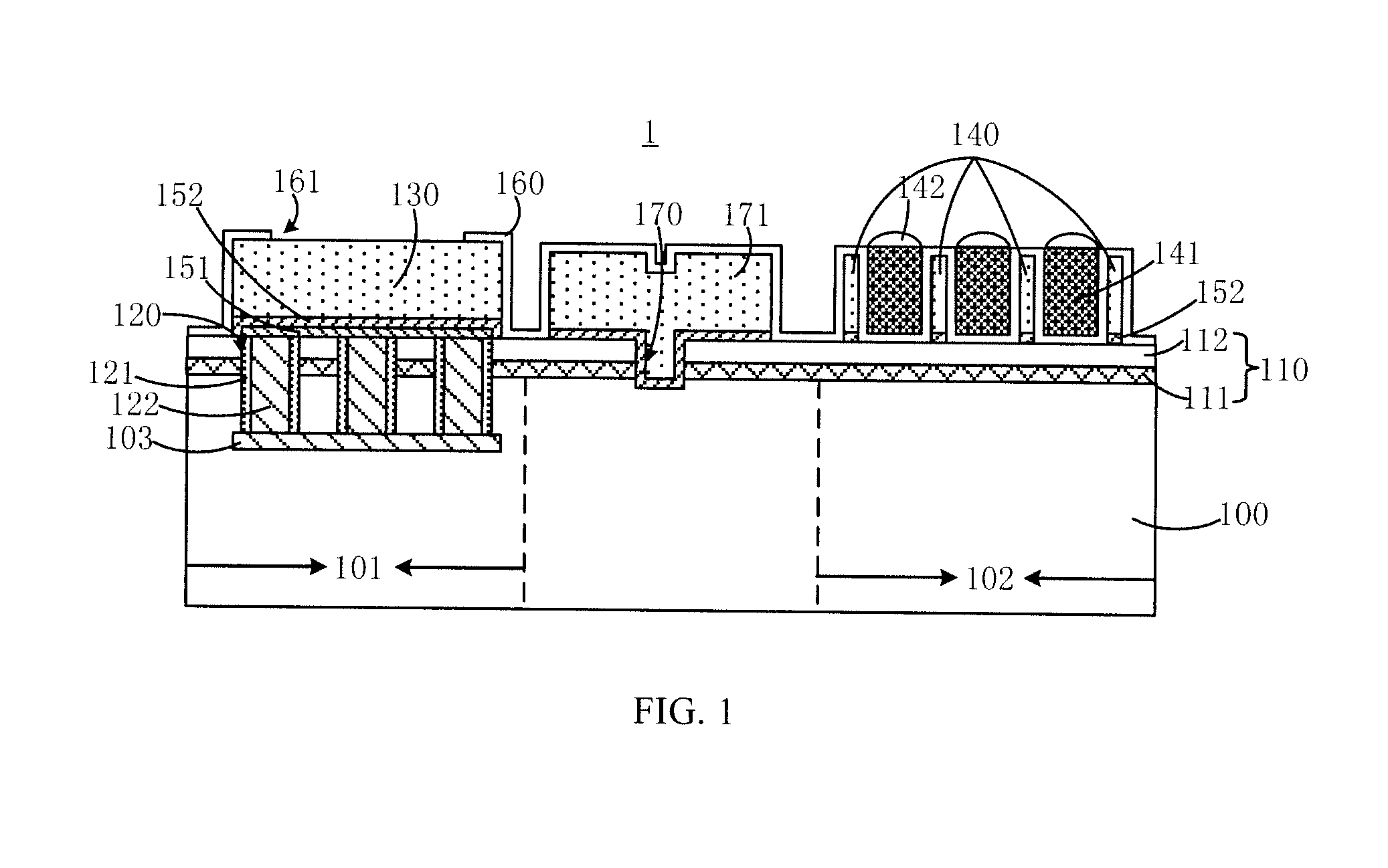
[0007]It is therefore an objective of the present invention to provide a method of fabricating a semiconductor structure, which is capable of simplifying semiconductor device fabrication processes (e.g., fabrication processes of CMOS sensors), improving production throughput, reducing production cost, and enhancing light absorption efficiency.
[0022]As described above, the method of the present invention provides the following advantages over the conventional methods.
[0023]Firstly, as the pad is connected to the connecting layer by the conductive structure and the pad and the metal structure are formed from the same metal layer, the advantages of process simplification, throughput improvement and cost reduction can be achieved by simultaneously fabricating the pad and the metal structure through forming a single metal layer and performing thereon a selective etching process.
[0024]Secondly, the only element disposed between the metal structure and the substrate is the protective insulating layer, which is particular beneficial for the applications where the metal structure is implemented as one or more light-blocking layers for optical filters disposed between the light-blocking layers, because this makes the protective insulating layer the only element disposed between the optical filters and the substrate and thus enables paths between the optical filters and corresponding photodiodes to be only intervened by the protective insulating layer but no protective layer for the pad, thereby enhancing light absorption efficiency of the CMOS sensor.

Problems solved by technology

However, as the light-blocking layers and the pad are conventionally formed in different processes using different techniques, the sensor fabrication process is associated with high complexity and cost and suffers from a low throughput.
Another deficiency of the conventional CMOS sensor is that a protection layer for the pad, which causes reduction of light absorption, intervenes between the optical filters and the photodiodes.

Method used


Image

  • Method of fabricating semiconductor structure
  • Method of fabricating semiconductor structure
  • Method of fabricating semiconductor structure

Examples


Embodiment Construction

[0028]The semiconductor structure and the method of fabricating the structure, of the present invention, will be described in greater detail in the following description which demonstrates preferred embodiments of the invention, in conjunction with the accompanying drawings. Those of skill in the art should, in light of the present disclosure, appreciate that many changes can be made in the specific embodiments disclosed herein and still obtain the same beneficial results. Therefore, the following description should be construed as the illustrative of the principles of the present invention, and not providing limitations thereto.

[0029]For simplicity and clarity of illustration, not all features of the specific embodiments are described. Additionally, descriptions and details of well-known functions and structures are omitted to avoid unnecessarily obscuring the invention. The development of any specific embodiment of the present invention includes specific decisions made to achieve ...


PUM

PropertyMeasurementUnit
thicknessaaaaaaaaaa
thicknessaaaaaaaaaa
thicknessaaaaaaaaaa

Abstract

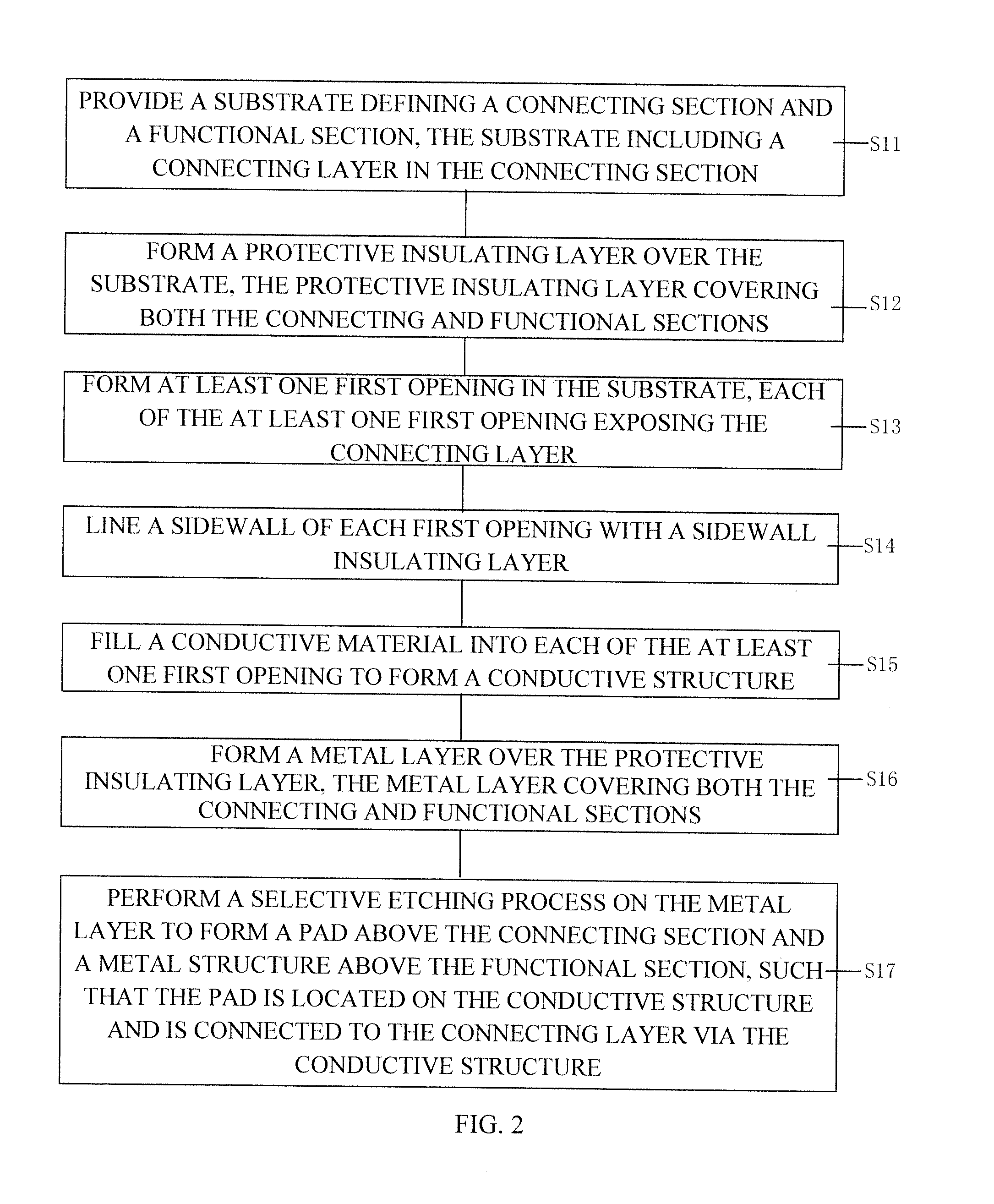
A method of fabricating a semiconductor structure is disclosed, in which a pad above a connecting section and metal structures above a functional section are formed from the same metal layer. This design enables the simultaneous formation of the pad and the metal structures by forming a single metal layer and performing thereon a selective etching process, thereby leading to the advantages of process simplification, throughput improvement and cost reduction.

Description

CROSS-REFERENCES TO RELATED APPLICATIONS[0001]This application claims the priority of Chinese patent application number 201410243358.7, filed on Jun. 3, 2014, the entire contents of which are incorporated herein by reference.TECHNICAL FIELD[0002]The present invention relates generally to semiconductor device fabrication, and in particular, to a method of fabricating a semiconductor structure.BACKGROUND[0003]With the development of multimedia technology, digital still cameras, digital video cameras and mobile phones with camera functions have gained increasing popularity among consumers. In addition to their pursuit for the miniaturization of these devices, customers are also demanding for an increasing improvement in the quality (i.e., clarity) of images captured by such devices. On the other hand, whether such a device could capture a high imaging quality heavily depends on what components the device incorporates. In particular, the imaging quality of a camera is determined by an i...

Claims


Application Information

Patent Timeline
Patent Type & Authority Applications(United States)
IPC IPC(8): H01L27/146
CPCH01L27/14685H01L21/743H01L23/485H01L27/14621H01L27/14623H01L27/14627H01L27/14636H01L27/14643H01L27/14687H01L21/28132H01L21/76877H01L23/481H01L24/83H01L27/14625
Inventor XING, JIAMINGYE, JINGGAO, XIFENGSHI, ZHETIAN
Owner OMNIVISION TECH (SHANGHAI) CO LTD
Learn More