
Superlattice photodetector thinned with improved performance and method of manufacturing the same

a superlattice photodetector and performance technology, applied in the direction of capacitors, radiation control devices, semiconductor devices, etc., can solve the problem of deteriorating performance of superlattice photodetectors

Pending Publication Date: 2022-05-12
KOREA ADVANCED INST OF SCI & TECH
View PDF13 Cites 0 Cited by
  • Summary
  • Abstract
  • Description
  • Claims
  • Application Information

AI Technical Summary

Benefits of technology

This patent is about improving the performance of a thin superlattice photodetector by increasing its light absorption efficiency. This can be achieved by adding a construction to the absorption layer that enhances light absorption, while reducing dark current and improving quantum efficiency. Additionally, the capacitor layer in the superlattice photodetector can be increased to increase its charge integrated capacity, resulting in improved performance even at a thinner thickness. Overall, the patent allows for improved performance and a thinner superlattice photodetector.

Problems solved by technology

Accordingly, in order to implement a superlattice photodetector having a reduced size, if the thickness of the absorption layer becomes thin, performance of the superlattice photodetector is also deteriorated.

Method used


Image

  • Superlattice photodetector thinned with improved performance and method of manufacturing the same
  • Superlattice photodetector thinned with improved performance and method of manufacturing the same
  • Superlattice photodetector thinned with improved performance and method of manufacturing the same

Examples


Embodiment Construction

[0017]While illustrative embodiments have been illustrated and described, it will be appreciated that various changes can be made therein without departing from the spirit and scope of the disclosure.

[0018]Hereinafter, various embodiments of this document are described with reference to the accompanying drawings.

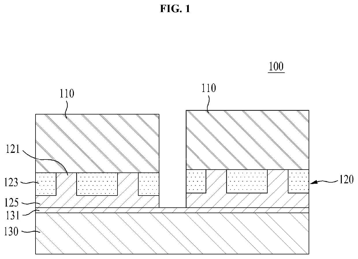
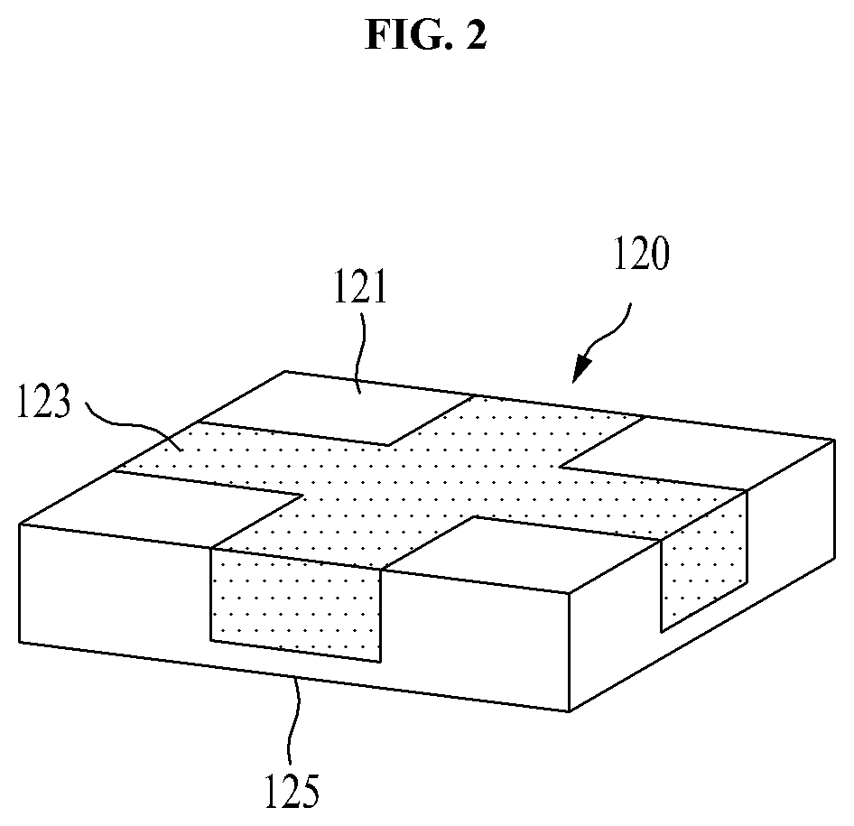
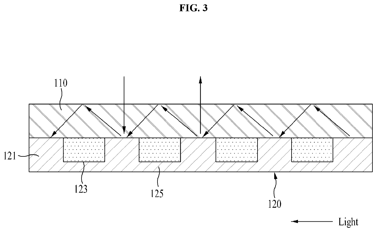
[0019]FIG. 1 is a diagram illustrating a superlattice photodetector 100 according to first embodiments. FIG. 2 is a perspective view illustrating a waveguide layer 120 of FIG. 1. FIG. 3 is a diagram for describing an operating characteristic of the waveguide layer 120 of FIG. 1.

[0020]Referring to FIG. 1, the superlattice photodetector 100 according to the first embodiments may include an absorption layer 110, the waveguide layer 120, and a circuit layer 130.

[0021]The absorption layer 110 may absorb incident light. Furthermore, the absorption layer 110 may generate an optical signal with respect to the absorbed light. In this case, the absorption layer 110 may be implemented ...


PUM

PropertyMeasurementUnit
dielectricaaaaaaaaaa
frequency bandaaaaaaaaaa
thicknessaaaaaaaaaa

Abstract

Various embodiments relate to a superlattice photodetector and a method of manufacturing the same. The superlattice photodetector includes an absorption layer for absorbing incident light and a waveguide layer coupled with the absorption layer and enabling the incident light to be waveguided within the absorption layer. The waveguide layer may include a periodic structure in which a plurality of metal patterns and a plurality of dielectric patterns are repeatedly arranged. According to various embodiments, the superlattice photodetector can be thinned while having improved performance.

Description

CROSS-REFERENCES TO RELATED APPLICATIONS[0001]This application is based on and claims priority under 35 U.S.C. 119 to Korean Patent Application No. 10-2020-0151149, filed on Nov. 12, 2020 in the Korean intellectual property office, the disclosures of which are herein incorporated by reference in their entireties.TECHNICAL FIELD[0002]Various embodiments relate to a superlattice photodetector thinned with improved performance and a method of manufacturing the same.BACKGROUND OF THE DISCLOSURE[0003]In general, a superlattice photodetector includes an absorption layer having a superlattice structure, and detects light having a desired frequency band by absorbing the light through the absorption layer. In this case, the thickness of the absorption layer is an important factor to determine performance of the superlattice photodetector. For example, as the thickness of the absorption layer becomes thick, a noise equivalent temperature difference (NETD) characteristic of the superlattice ph...

Claims


Application Information

Patent Timeline
Patent Type & Authority Applications(United States)
IPC IPC(8): H01L31/0352H01L31/0232H01L27/144H01L49/02H01L31/18H10N97/00
CPCH01L31/035236H01L31/0232H01L31/186H01L28/40H01L27/1443H01L31/02327H01L31/08
Inventor KIM, SANGHYEONGEUM, DAEMYEONGAHN, SEUNGYEOPLIM, JINHA
Owner KOREA ADVANCED INST OF SCI & TECH
Learn More