
Schottky device

a technology of schottky barriers and devices, which is applied in the direction of semiconductor devices, basic electric elements, electric devices, etc., to achieve the effect of reasonable production cost and high yield

Inactive Publication Date: 2014-07-01
QUNANO
View PDF16 Cites 0 Cited by
  • Summary
  • Abstract
  • Description
  • Claims
  • Application Information

AI Technical Summary

Benefits of technology

This invention enables the fabrication of Schottky diodes with high yield using a material system and technique. It also increases the possibility of integrating standard Si micro electronic devices and wide-bandgap semiconductor two-terminal devices on the same substrate. The use of a standard Si substrate and the integration of high performance nanowire devices with standard semiconductor electronics offer the possibility of full integration on a standard Si-substrate while keeping production cost on a reasonable level.

Problems solved by technology

The prior art has drawbacks with regard to being able to produce wide bandgap Schottky diodes.

Method used


Image

  • Schottky device
  • Schottky device
  • Schottky device

Examples


Embodiment Construction

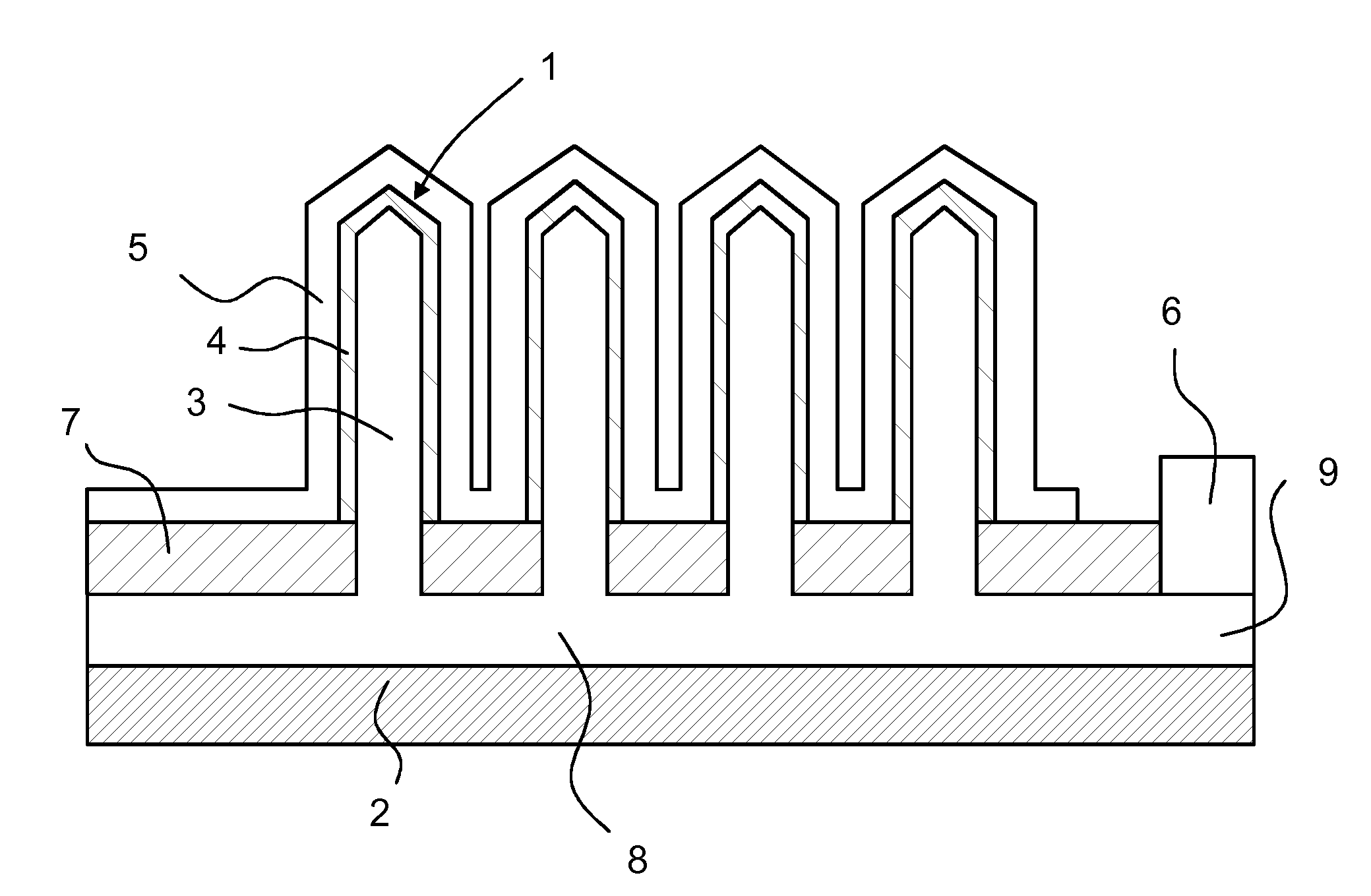
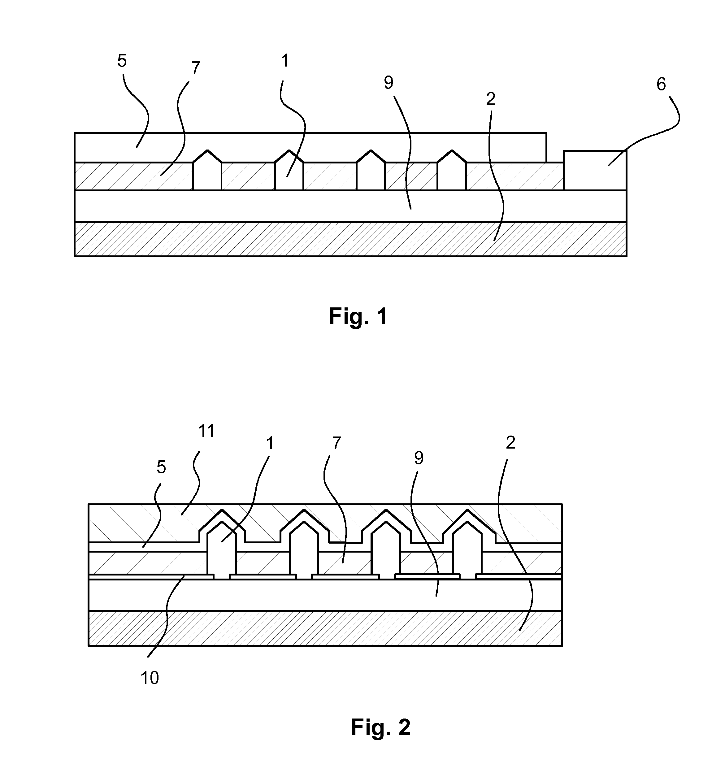
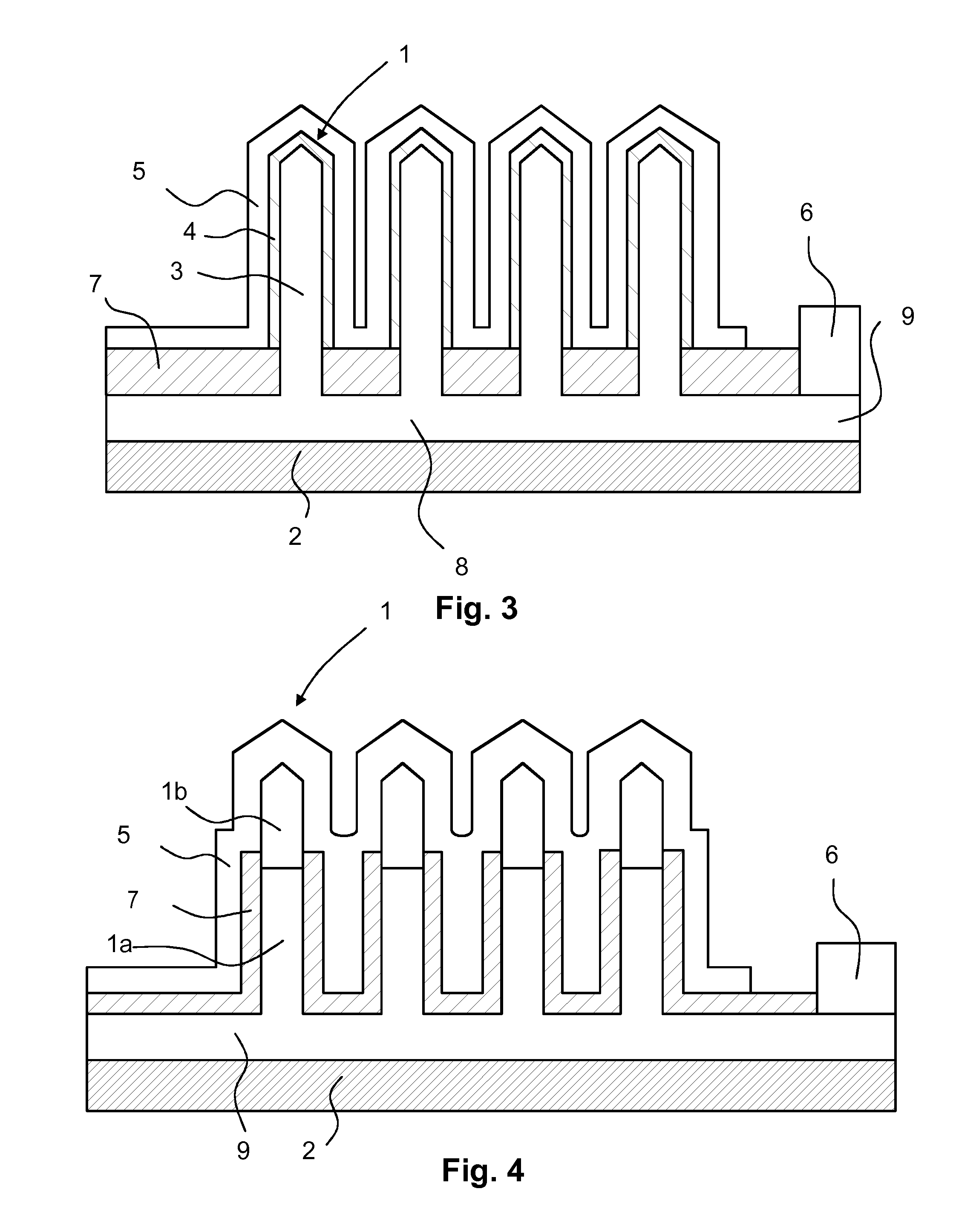
[0031]The embodiments to be described in the following are all based on the use of nanowires and for the purpose of this application the term nanowire is to be interpreted as a structure having a shape that is of nanometer dimensions in its width or diameter. Such structures are commonly also referred to as nanowhiskers, one-dimensional nano-elements, nanorods, etc. However, nanowires can also benefit from some of the unique properties of nanowires without having a non-elongated shape. By way of example, non-elongated nanowires, e.g. of pyramidal shape or as thin as only a few epitaxial layers, can be formed on a substrate material having relatively large defect density in order to provide defect-free templates for further processing.

[0032]The nanowires of the present invention are grown on a substrate, often referred to as wafer in the field of microelectronics. The substrate may include one or more surface layers on the surface thereof. These layers are commonly referred to as a b...


PUM

PropertyMeasurementUnit
voltageaaaaaaaaaa
diameteraaaaaaaaaa
diameteraaaaaaaaaa

Abstract

A device includes a Schottky barrier formed by a metal-semiconductor junction between a semiconductor nanowire and a metal contact. The metal contact at least partly encloses a circumferential area of each nanowire along the length thereof. The nanowire includes a low doped region that is part of the metal-semiconductor junction. The device can be fabricated using a method where two different growth modes are used, the first step including axial growth from a substrate giving a suitable template for formation of the metal-semiconductor junction, and the second step including radial growth enabling control of the doping levels in the low doped region.

Description

CROSS-REFERENCE TO OTHER APPLICATIONS[0001]This application is a national phase application under 35 U.S.C. §371 of international application PCT / SE2010 / 050332 (filed Mar. 25, 2010) which claims priority to Swedish Application 0950186-7 (filed Mar. 25, 2009).TECHNICAL FIELD OF THE INVENTION[0002]The present invention relates to devices comprising Schottky barriers. In particular the invention relates to devices comprising a Schottky barrier formed by a metal-semiconductor junction between a semiconductor nanowire and a metal contact.BACKGROUND OF THE INVENTION[0003]Among metal-semiconductor contacts, there are two main groups: ohmic contacts and Schottky contacts. An ohmic contact is referred to as a metal-semiconductor contact that has negligible contact resistance relative to the series resistance of the semiconductor and a small voltage drop over the metal-semiconductor contact as compared to the total voltage drop across a device comprising the metal-semiconductor contact. A Sch...

Claims


Application Information

Patent Timeline
Patent Type & Authority Patents(United States)
IPC IPC(8): H01L29/47
CPCH01L29/872H01L29/0665H01L29/0673H01L29/0676H01L29/66143H01L29/06
Inventor KONSEK, STEVEN
Owner QUNANO
Learn More