
Microfabricated neural probes and methods of making same

a neural probe and micro-fabricated technology, applied in the field of micro-electromechanical systems, can solve the problems of limited spatial resolution of micro-machined neural probes and more expensive probes than desired

Active Publication Date: 2014-06-10
CALIFORNIA INST OF TECH
View PDF14 Cites 27 Cited by
  • Summary
  • Abstract
  • Description
  • Claims
  • Application Information

AI Technical Summary

Benefits of technology

The invention is about a neural probe that has small recording electrodes made of nanometers (less than 1 micrometer) in width and 10 micrometers or less in distance between them. Another embodiment of the invention is a neural probe with microfabricated recording electrodes located on a flexible polymer cantilever. These improvements enable the probe to more accurately and precisely measure the activity of neural cells.

Problems solved by technology

The micromachined neural probes have limited spatial resolution.
Furthermore, the present inventors realized that these probes are more expensive than desired because they are made using expensive silicon processing steps, such as reactive ion etching (RIE) and plasma-enhanced chemical vapor deposition (PECVD).

Method used


Image

  • Microfabricated neural probes and methods of making same
  • Microfabricated neural probes and methods of making same
  • Microfabricated neural probes and methods of making same

Examples


first embodiment

1. First Embodiment

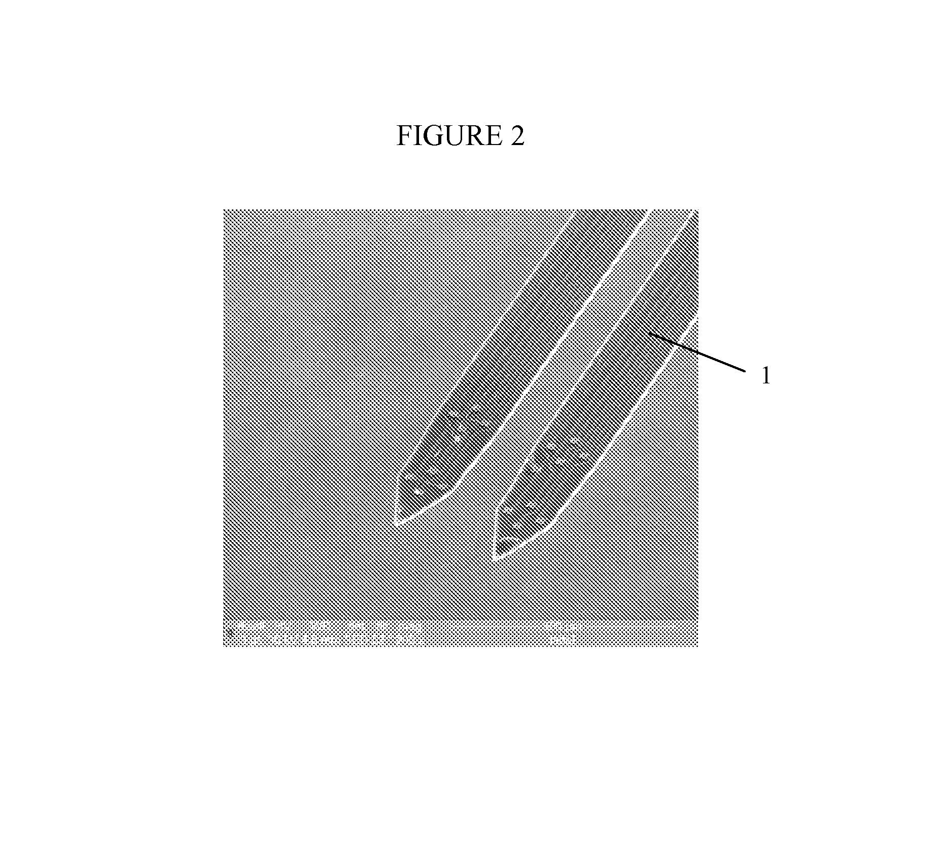
[0051]In a first embodiment of the invention, the present inventors have developed a method to fabricate a neural probe which contains a plurality of nanoscale recording electrodes. Preferably, the recording electrodes have a width of 1 micron or less, such as about 0.1 to about 0.8 microns, form example about 0.3 to about 0.5 microns. It should be noted that while the electrodes preferably have a round cross section where the width of the electrodes refers to their diameter, they may also have polygonal or irregular cross section, where the width refers to the maximum width of the electrodes. The electrodes may have any suitable height, such as 6 microns or less, for example 2 to 5 microns.

[0052]Preferably, a distance between adjacent recording electrodes is 10 microns or less, such as 1 to 4 microns, for example. The probe electrode density is preferably about 1 / 10 nm squared to about 1 / 50 nm squared. The electrode width and spacing is designed to allow the prob...

second embodiment

2. Second Embodiment

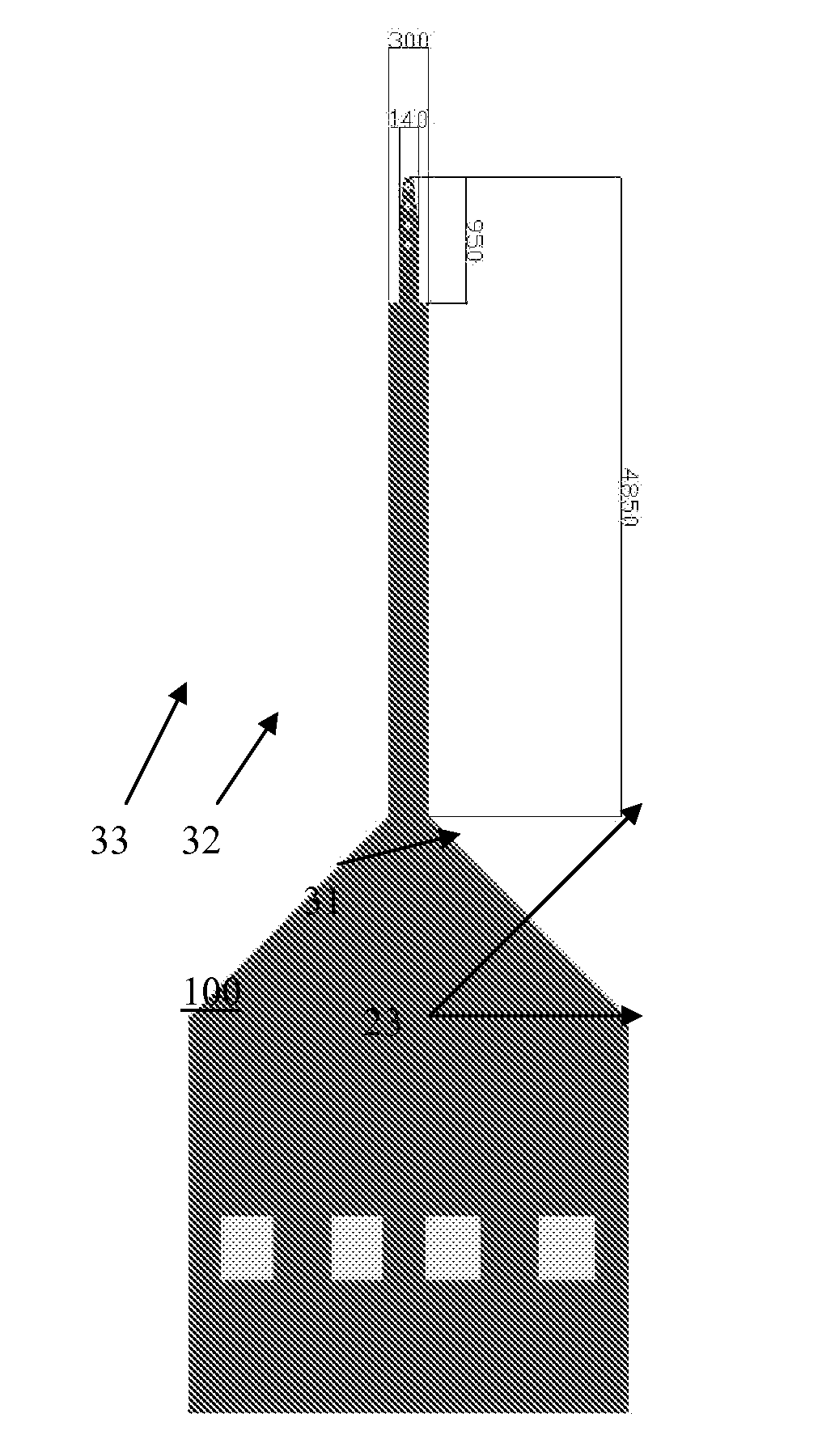
[0062]The second embodiment provides a neural probe comprising a plurality of microfabricated recording electrodes located on a polymer base material. Preferably, the recording pads containing the electrodes are located on and / or are partially encapsulated in a flexible cantilever shaped polymer structure. The preferred polymer materials are SU-8 and parylene. However, other materials may also be used. The second embodiment also provides a method of making a neural probe which includes forming a polymer support structure and forming conductors encapsulated in the polymer support structure. The conductors electrically connect exposed electrically addressable metal pads to a plurality of recording electrodes to form the neural probe.

[0063]In a first aspect of the second embodiment, the electrodes are located on the SU-8 polymer material. SU-8 is a negative tone, near UV photo-resist. Its properties allow building s structure from 0.5 μm to 300 μm thick. The advanta...


PUM


Abstract

An embodiment of the invention provides a neural probe containing a plurality of nanoscale recording electrodes. The recording electrodes have a width of 1 micron or less and a distance between adjacent recording electrodes is 10 microns or less. Another embodiment of the invention provides a neural probe comprising a plurality of microfabricated recording electrodes located on a polymer base material, such as a flexible polymer cantilever.

Description

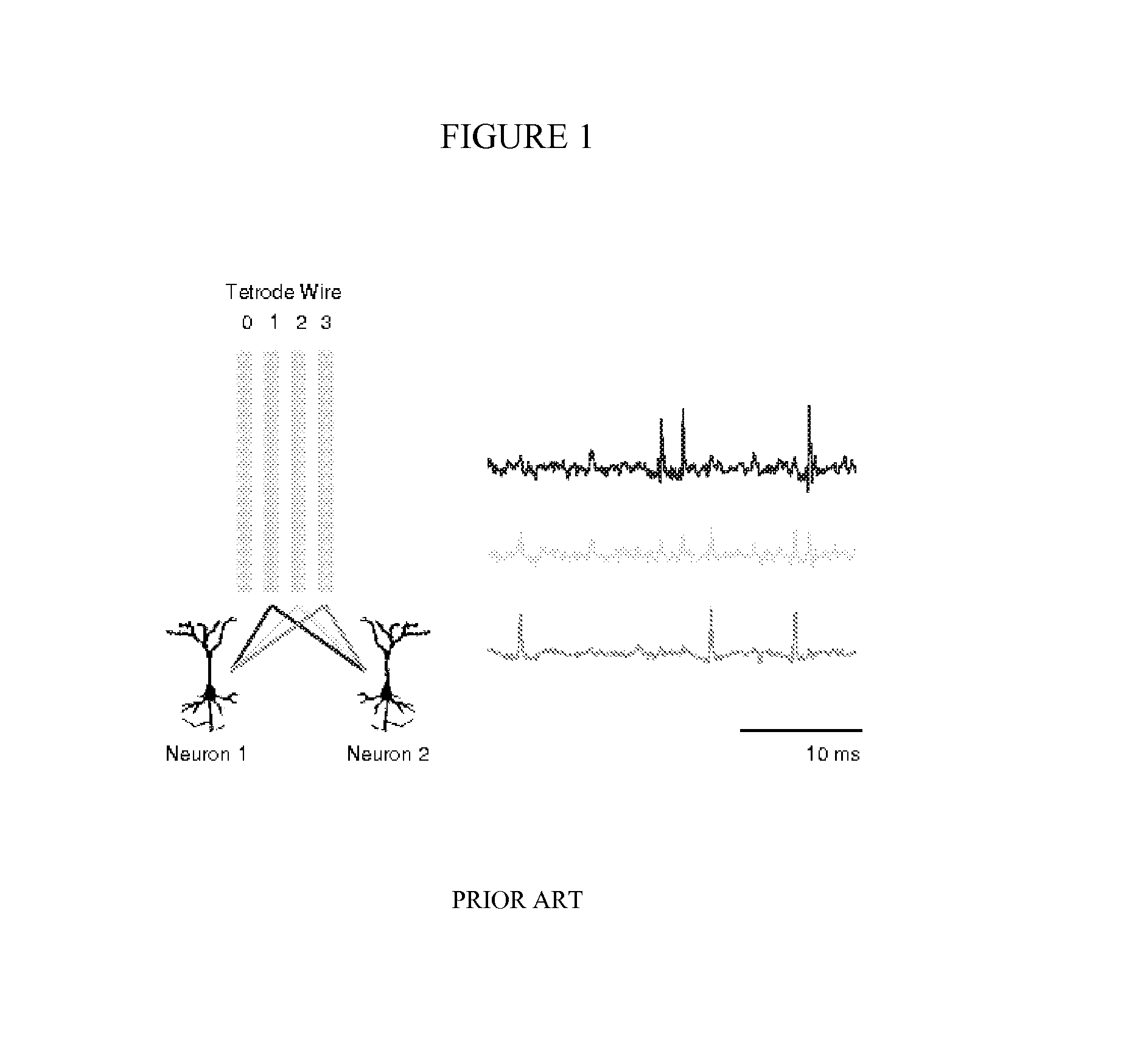
[0001]This application claims benefit of priority of U.S. Provisional Application Ser. No. 60 / 575,991 filed Jun. 1, 2004, which is incorporated herein by reference in its entirety.BACKGROUND OF THE INVENTION[0002]1. Field of the Invention[0003]The invention is related to micro-electro-mechanical systems (MEMS) and methods of making these systems.[0004]2. Description of the Prior Art[0005]In neurobiology, to study the central nervous system, electro physiologists use electrodes (referred to herein as recording electrodes) placed in the extra-cellular medium to record the activity of multiples neurons simultaneously. The variation of the local electrical potential is detected or recorded due to the action potentials (spikes) occurring in the surrounding neurons. By using more than one electrode, it is then possible to distinguish action potentials coming from different neurons due to the variation of the shape of the spike while traveling in the extracellular media. This way, each neu...

Claims


Application Information

Patent Timeline
Patent Type & Authority Patents(United States)
IPC IPC(8): A61N1/00A61B5/04A61N1/05
CPCA61B2562/028A61B5/685A61B5/04001A61N1/05B82Y15/00A61B5/24
Inventor TANG, HONGXINGROUKES, MICHAEL L.RENAUD, RICHARD
Owner CALIFORNIA INST OF TECH
Learn More