
Single event latch-up prevention techniques for a semiconductor device

a single-event latchup and semiconductor technology, applied in the direction of semiconductor devices, electrical equipment, thyristor, etc., can solve the problems of sel induced current destroying semiconductor device components, permanent damage to semiconductor devices, and seus affecting semiconductor devices in the atmospher

Inactive Publication Date: 2014-04-01
NXP USA INC
View PDF4 Cites 7 Cited by
  • Summary
  • Abstract
  • Description
  • Claims
  • Application Information

AI Technical Summary

Benefits of technology

The patent text discusses techniques for preventing single-event latch-up (SEL) in semiconductor devices. SEL is a type of damage caused by ions or electromagnetic radiation that can permanently damage a semiconductor device. The text describes the causes and effects of SEL, as well as conventional methods for preventing it, such as current limiters. The technical effect of the patent is to provide new methods for preventing SEL in semiconductor devices, particularly in the context of complementary metal-oxide semiconductor technology.

Problems solved by technology

In contrast, a single-event latch-up (SEL), a single-event gate rupture (SEGR), and / or a single-event burnout (SEB) may permanently damage a semiconductor device.
During an SEL, an SEL induced current may destroy components of a semiconductor device if the SEL induced current is not limited and promptly removed.
At sub-micron geometries, SEUs may adversely affect semiconductor devices in the atmosphere.
Trace amounts of radioactive elements in integrated circuit (chip) packages may also cause SELs.
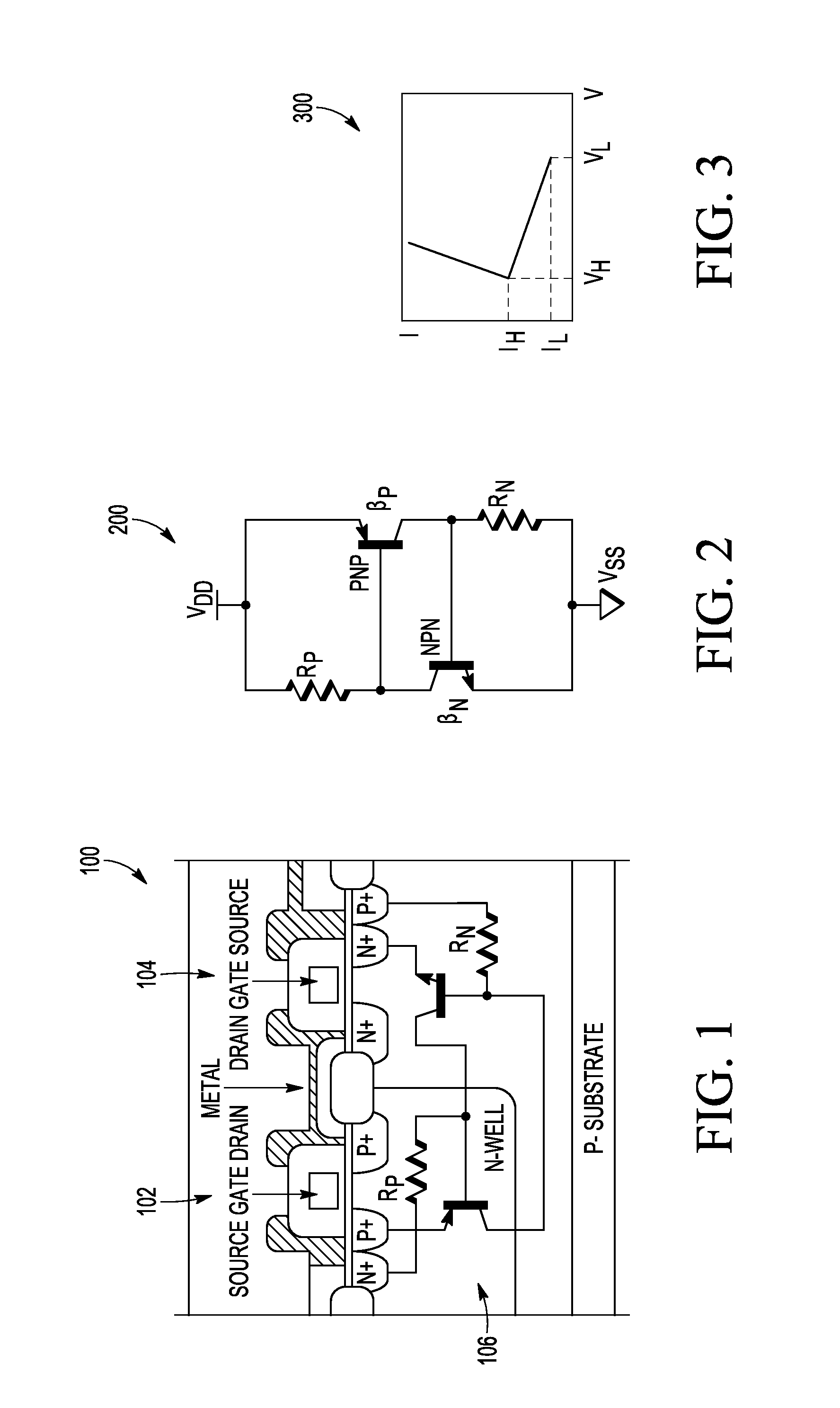
The parasitic BJT devices may create problems when triggered.
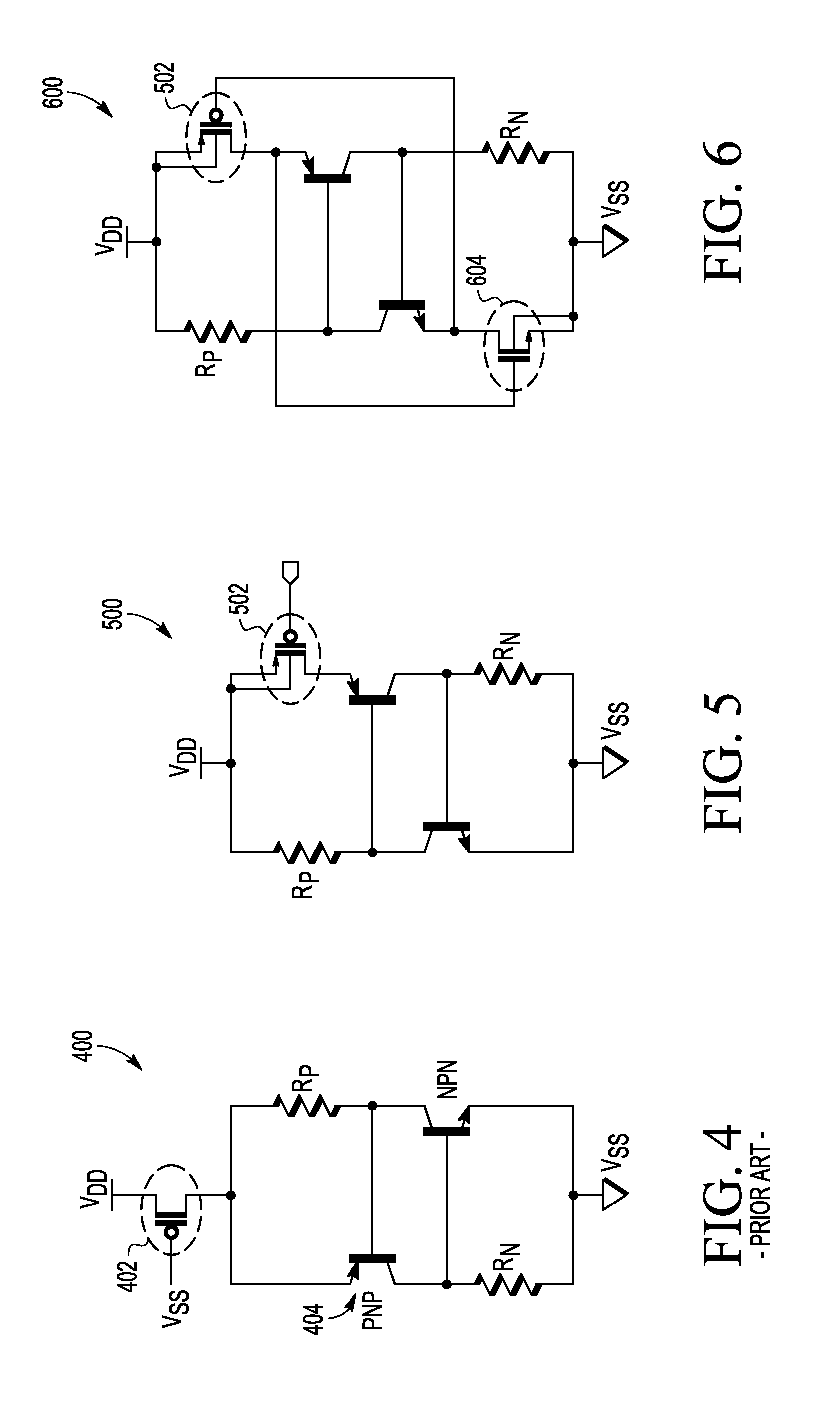
For example, triggering the parasitic BJT devices may lead to shorting power (VDD) and ground (VSS) lines, which may result in destruction of an associated chip or an associated electronic system failure that can only be resolved by power-down.

Method used


Image

  • Single event latch-up prevention techniques for a semiconductor device
  • Single event latch-up prevention techniques for a semiconductor device
  • Single event latch-up prevention techniques for a semiconductor device

Examples


Embodiment Construction

[0026]In the following detailed description of exemplary embodiments of the invention, specific exemplary embodiments in which the invention may be practiced are described in sufficient detail to enable those skilled in the art to practice the invention, and it is to be understood that other embodiments may be utilized and that logical, architectural, programmatic, mechanical, electrical and other changes may be made without departing from the spirit or scope of the present invention. The following detailed description is, therefore, not to be taken in a limiting sense, and the scope of the present invention is defined only by the appended claims and their equivalents. As may be used herein, the term ‘coupled’ includes a direct electrical connection between elements or components and an indirect electrical connection between elements or components achieved using one or more intervening elements or components.

[0027]The present disclosure is generally directed to single-event latch-up...


PUM


Abstract

A technique for addressing single-event latch-up (SEL) in a semiconductor device includes determining a location of a parasitic silicon-controlled rectifier (SCR) in an integrated circuit design of the semiconductor device. In this case, the parasitic SCR includes a parasitic pnp bipolar junction transistor (BJT) and a parasitic npn BJT. The technique also includes incorporating a first transistor between a first power supply node and an emitter of the parasitic pnp BJT in the integrated circuit design. The first transistor includes a first terminal coupled to the first power supply node, a second terminal coupled to the emitter of the parasitic pnp BJT, and a control terminal. The first transistor is not positioned between a base of the pnp BJT and the first power supply node. The first transistor limits current conducted by the parasitic pnp bipolar junction transistor following an SEL.

Description

BACKGROUND[0001]1. Field[0002]This disclosure relates generally to single-event latch-up and, more specifically, to techniques for preventing single-event latch-up of a semiconductor device.[0003]2. Related Art[0004]A single-event upset (SEU) is a change of state caused by ions or electromagnetic radiation striking a sensitive node in a semiconductor device, such as a node in a microprocessor, memory, or power transistor. In general, the state change is a result of free charge created by ionization in or close to a sensitive node of a logic element (e.g., a node of a memory bit cell). The error in semiconductor device output or operation due to a high energy particle strike is often referred to as a soft error upset or SEU.[0005]Typically, an SEU has not permanently damaged functionality of a semiconductor device. In contrast, a single-event latch-up (SEL), a single-event gate rupture (SEGR), and / or a single-event burnout (SEB) may permanently damage a semiconductor device. An SEL m...

Claims


Application Information

Patent Timeline
Patent Type & Authority Patents(United States)
IPC IPC(8): H01L21/332
CPCG06F17/50H01L27/0921H01L27/06
Inventor YANG, JIANANBURNETT, JAMES D.GARNI, BRAD J.LISTON, THOMAS W.PHAM, HUY VAN
Owner NXP USA INC
Learn More