
Techniques for gate workfunction engineering to reduce short channel effects in planar CMOS devices

a technology of gate workfunction and gate workfunction, which is applied in the direction of semiconductor devices, electrical devices, transistors, etc., can solve the problems of non-uniform channel doping, and achieve the effect of reducing short channel effects

Active Publication Date: 2014-03-18
GLOBALFOUNDRIES U S INC
View PDF20 Cites 16 Cited by
  • Summary
  • Abstract
  • Description
  • Claims
  • Application Information

AI Technical Summary

Benefits of technology

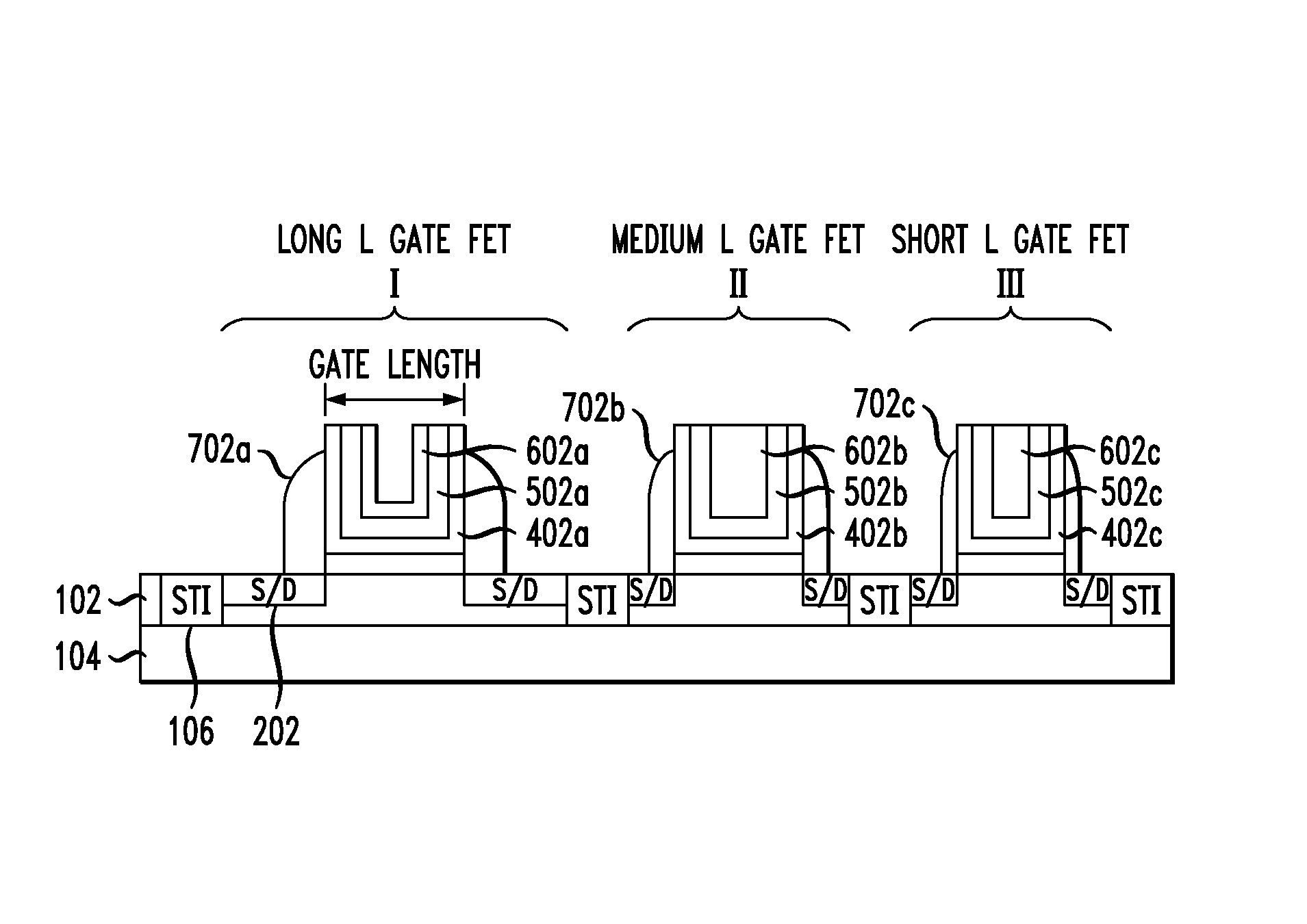
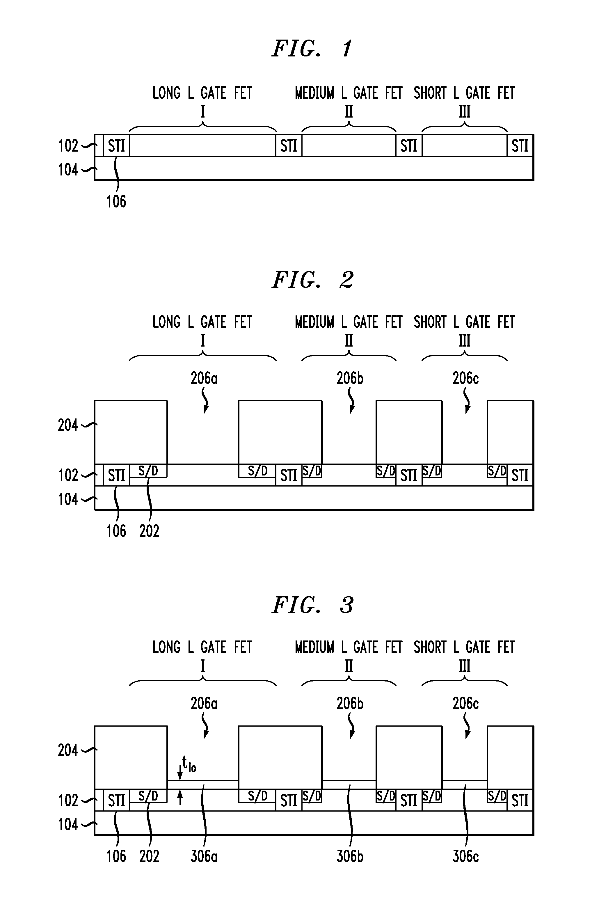
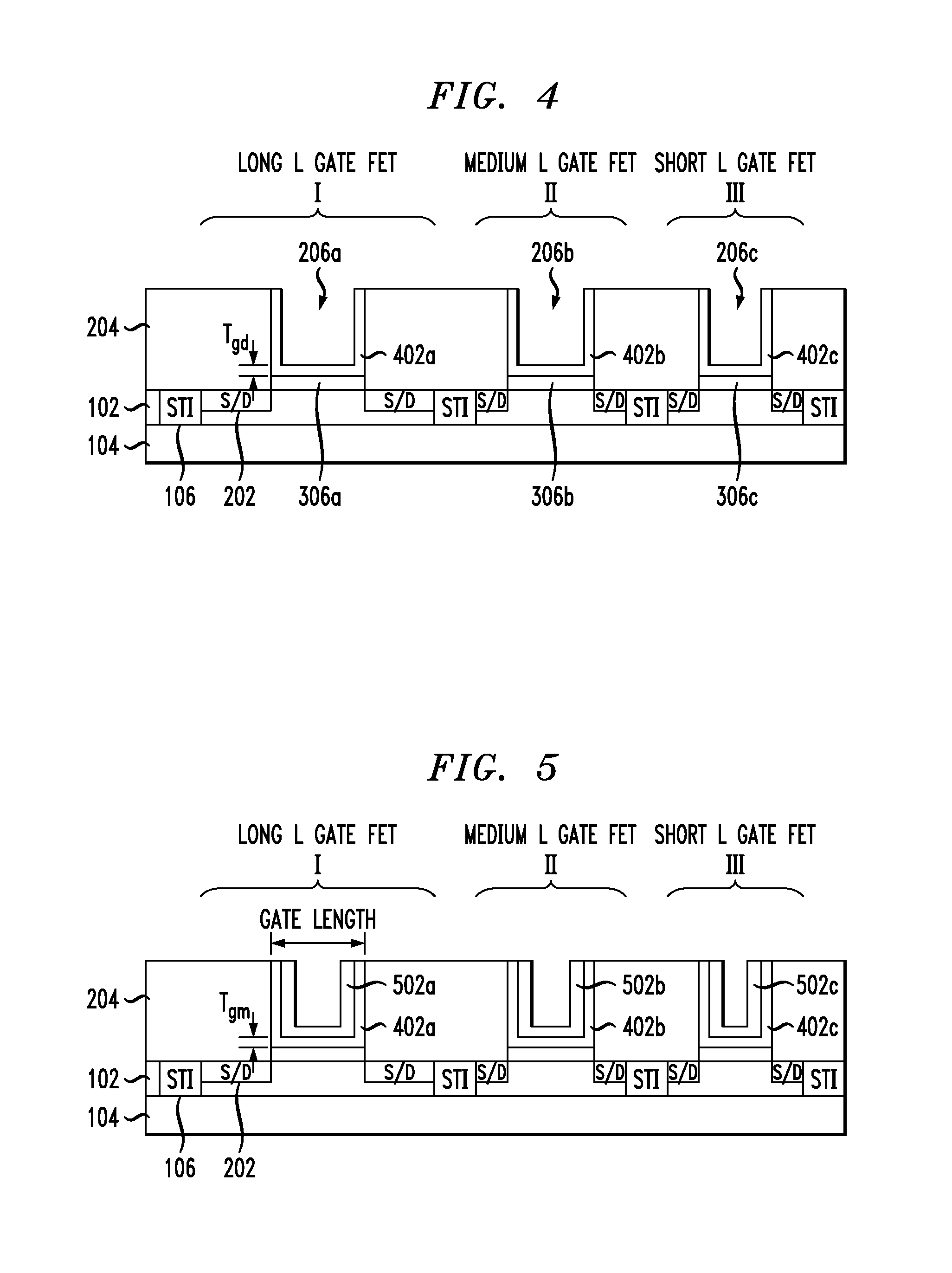
The present invention provides techniques for improving the performance of CMOS devices by engineering the gate workfunction using a workfunction setting material. This involves depositing a conformal gate dielectric layer, a conformal gate metal layer, and a conformal workfunction setting metal layer in each trench where a gate stack is to be formed. The volume of the deposited layers is proportional to the length of the gate stack being formed. This technique helps to reduce short channel effects in CMOS devices and enhance their performance.

Problems solved by technology

This issue has exacerbated several other scaling parameters, such as the distance between the metal contact and the gate.
Namely, with CMOS devices, non-uniform channel doping is typically present where the source and drain regions of the device are more heavily doped (i.e., halo doping to reduce the depletion regions).

Method used


Image

  • Techniques for gate workfunction engineering to reduce short channel effects in planar CMOS devices
  • Techniques for gate workfunction engineering to reduce short channel effects in planar CMOS devices
  • Techniques for gate workfunction engineering to reduce short channel effects in planar CMOS devices

Examples


Embodiment Construction

[0015]Provided herein are techniques for the use of a work function setting material to reduce short channel effects in planar complementary metal-oxide semiconductor (CMOS) devices. An amount of the work function setting material employed will be continually modulated as a function of channel length. The present techniques may be applied to planar CMOS (bulk, partially depleted silicon-on-insulator (PDSOI), fully depleted SOI (FDSOI), and extremely thin SOI (ETSOI) devices).

[0016]The present techniques are applicable in both gate-first and gate-last process flows. In general, a gate-first approach to planar CMOS device fabrication involves formation of the gate early in the process, and use of the gate to position the source and drain doping. The dopant implantation and activation process (which involves annealing) can however damage the gate materials. Thus, more recently a gate-last approach has been investigated where a dummy gate is used in place of the traditional gate early i...


PUM


Abstract

Techniques for gate workfunction engineering using a workfunction setting material to reduce short channel effects in planar CMOS devices are provided. In one aspect, a method of fabricating a CMOS device includes the following steps. A SOI wafer is provided having a SOI layer over a BOX. A patterned dielectric is formed on the wafer having trenches therein present over active areas in which a gate stack will be formed. Into each of the trenches depositing: (i) a conformal gate dielectric (ii) a conformal gate metal layer and (iii) a conformal workfunction setting metal layer. A volume of the conformal gate metal layer and / or a volume of the conformal workfunction setting metal layer deposited into a given one of the trenches are / is proportional to a length of the gate stack being formed in the given trench. A CMOS device is also provided.

Description

FIELD OF THE INVENTION[0001]The present invention relates to planar complementary metal-oxide semiconductor (CMOS) devices, and more particularly, to techniques for gate workfunction engineering using a workfunction setting material to reduce short channel effects in planar CMOS devices.BACKGROUND OF THE INVENTION[0002]In current CMOS scaling, the scaling of the physical channel length has not kept up with other scaling parameters. This issue has exacerbated several other scaling parameters, such as the distance between the metal contact and the gate.[0003]A reverse short channel effect is a reduction in threshold voltage as the gate length increases. Namely, with CMOS devices, non-uniform channel doping is typically present where the source and drain regions of the device are more heavily doped (i.e., halo doping to reduce the depletion regions). As a result, in short channel length devices, the source and drain halo doping regions can overlap (also referred to as halo merging), th...

Claims


Application Information

Patent Timeline
Patent Type & Authority Patents(United States)
IPC IPC(8): H01L27/092
CPCH01L21/84H01L27/1203H01L21/823842H01L21/82385H01L29/66545H01L29/78
Inventor CHANG, JOSEPHINE B.LAUER, ISAACLIN, CHUNG-HSUNSLEIGHT, JEFFREY W.
Owner GLOBALFOUNDRIES U S INC
Learn More