
Soft error rate detector

a detector and error rate technology, applied in the field of soft error rate detectors, can solve problems such as soft errors, radiation-induced misbehavior, and integrated circuits

Active Publication Date: 2014-01-28
GLOBALFOUNDRIES US INC
View PDF4 Cites 22 Cited by
  • Summary
  • Abstract
  • Description
  • Claims
  • Application Information

AI Technical Summary

Benefits of technology

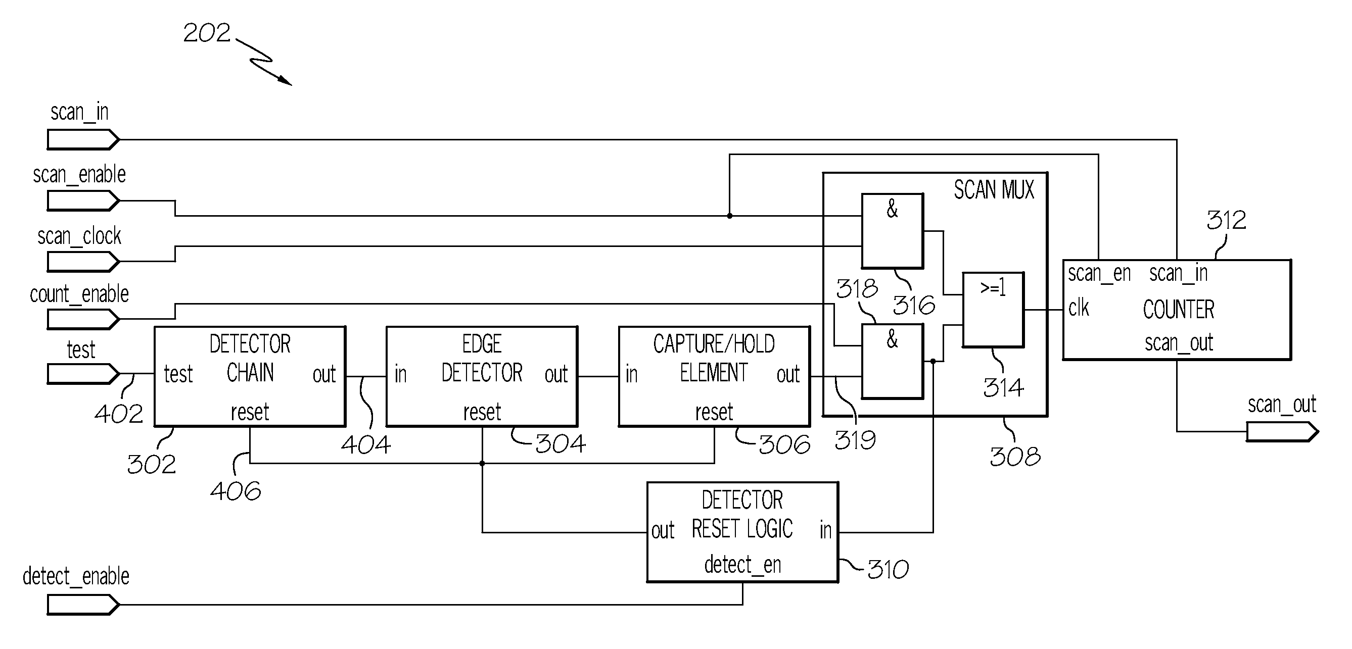
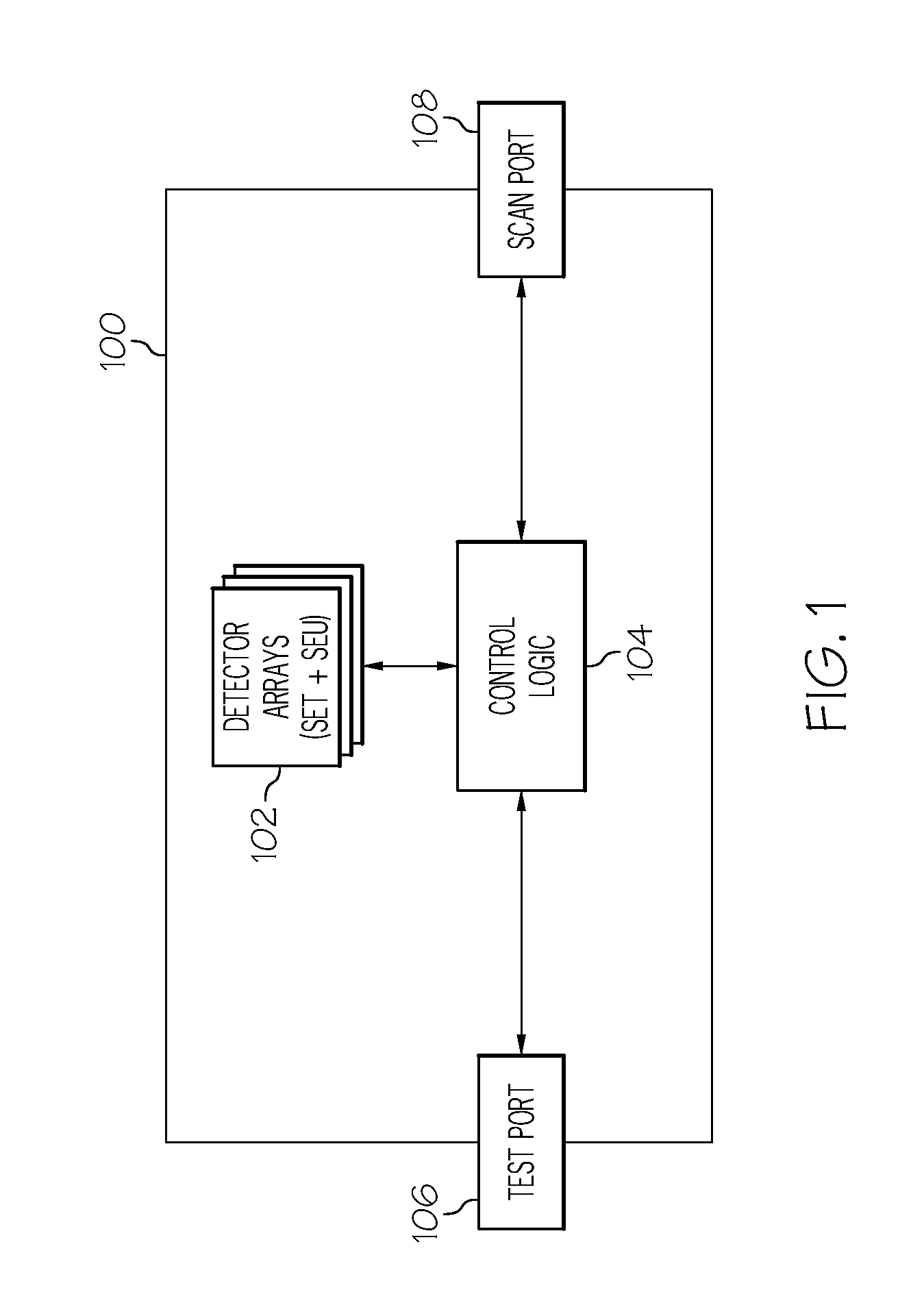
The patent text describes a soft error rate (SER) detector circuit that can detect both single event transients (SETs) and single event upsets (SEUs) using a combined test structure. The circuit includes multiple detector arrays with individual test structures for each array. The test structures have a persistent output state for detection of SETs. The circuit also includes logic elements to control the operation of the detector arrays. The technical effect of this invention is to provide a more efficient and effective means for detecting and measuring the soft error rate of semiconductor devices.

Problems solved by technology

Exposure of integrated circuits to nuclear radiation can trigger soft errors (radiation-induced misbehavior).
Consequently, such existing solutions are inefficient and costly.

Method used


Image

  • Soft error rate detector
  • Soft error rate detector
  • Soft error rate detector

Examples


Embodiment Construction

[0019]The following detailed description is merely illustrative in nature and is not intended to limit the embodiments of the subject matter or the application and uses of such embodiments. As used herein, the word “exemplary” means “serving as an example, instance, or illustration.” Any implementation described herein as exemplary is not necessarily to be construed as preferred or advantageous over other implementations. Furthermore, there is no intention to be bound by any expressed or implied theory presented in the preceding technical field, background, brief summary or the following detailed description.

[0020]The subject matter presented here relates to a semiconductor-based test device designed to detect and measure soft errors (e.g., soft error rate or SER), such as those induced by radiation, whether externally applied radiation or “internally” applied radiation caused by materials and elements of the device itself The test device leverages scanning techniques where a known ...


PUM


Abstract

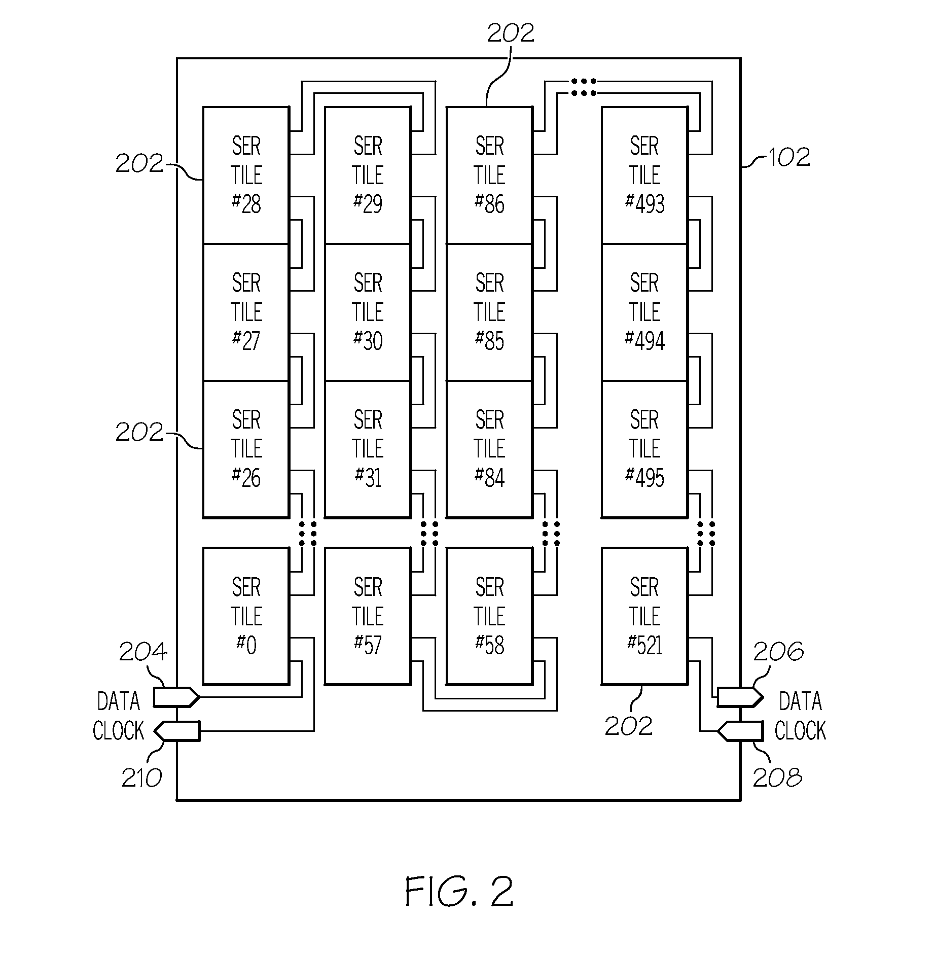
The soft error rate (SER) detector circuit presented here can be used to measure SER in combinatorial logic devices caused by radiation. The SER detector circuit includes a plurality of detector arrays coupled in series, and each having a plurality of SER test structures coupled in series. Each of the SER test structures includes a plurality of detector elements coupled in series. Each of the SER test structures is configured to detect single event transients (SETs) in a first operating mode and single event upsets (SEUs) in a second operating mode. The SER detector circuit also has control logic elements to control operation of the plurality of detector arrays.

Description

TECHNICAL FIELD[0001]Embodiments of the subject matter described herein relate generally to semiconductor devices. More particularly, embodiments of the subject matter relate to a semiconductor-based test structure for detecting soft errors induced by radiation.BACKGROUND[0002]Semiconductor devices, fabrication processes for manufacturing semiconductor devices, and associated test circuits and test structures are well known. On-chip test architectures are often used to check certain characteristics of a semiconductor device (such as a device that implements combinatorial or sequential logic) manufactured by a particular process. In this regard, the on-chip test structure is fabricated using the proposed manufacturing process, and with standard circuit modules, cell libraries, and the like. Consequently, the on-chip test structure can be exposed to controlled test conditions (e.g., temperature, radiation, electromagnetic interference) to determine how other devices fabricated in acco...

Claims


Application Information

Patent Timeline
Patent Type & Authority Patents(United States)
IPC IPC(8): G06F11/00G01R31/28
CPCG06F11/24
Inventor HAUFE, CHRISTIANPIKA, JENSWINKLER, JORG
Owner GLOBALFOUNDRIES US INC
Learn More