
Method and system for heterogeneous substrate bonding of waveguide receivers

a waveguide receiver and heterogeneous substrate technology, applied in semiconductor lasers, semiconductor/solid-state device details, instruments, etc., can solve the problem that silicon is not a direct bandgap material, and achieve good mechanical strength, good electrical conductivity, and sufficient compliance

Inactive Publication Date: 2013-12-17
SKORPIOS TECH
View PDF57 Cites 108 Cited by
  • Summary
  • Abstract
  • Description
  • Claims
  • Application Information

AI Technical Summary

Benefits of technology

This approach provides a bond with excellent mechanical strength, electrical conductivity, and optical transparency, allowing for reliable and efficient electrical and optical functionality across the bonded interface, overcoming the limitations of conventional techniques.

Problems solved by technology

On the other hand, silicon is not a direct bandgap materials.

Method used


Image

  • Method and system for heterogeneous substrate bonding of waveguide receivers
  • Method and system for heterogeneous substrate bonding of waveguide receivers
  • Method and system for heterogeneous substrate bonding of waveguide receivers

Examples


Embodiment Construction

[0020]Embodiments of the present invention relate to an apparatus and method that preferably uses a bonding stress for wafer bonding and utilizes an intermediate layer to facilitate the transition from silicon and the like to another material for optical coupling as well as electron transport. Embodiments of the present invention preferably incorporate low stress, low temperature wafer bonding known in the industry and preferably comprise a thin film intermediate layer for optical coupling as well electron transport.

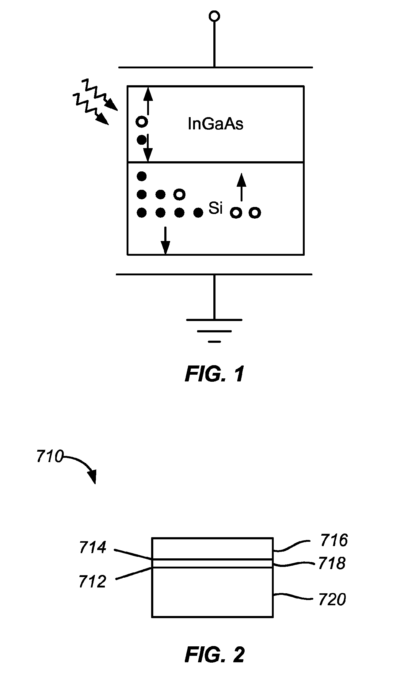
[0021]FIG. 1 illustrates an example of a photodiode with a low stress bond between a III-V substrate and a silicon substrate. FIG. 2 illustrates a bonded structure according to an embodiment of the present invention. As illustrated in FIG. 2, two interfaces 712 and 714 are provided. First interface 712 is positioned between a silicon substrate 720 and an intermediate layer 718. Second interface 714 is located between intermediate layer 718 and a second semiconductor laye...


PUM


Abstract

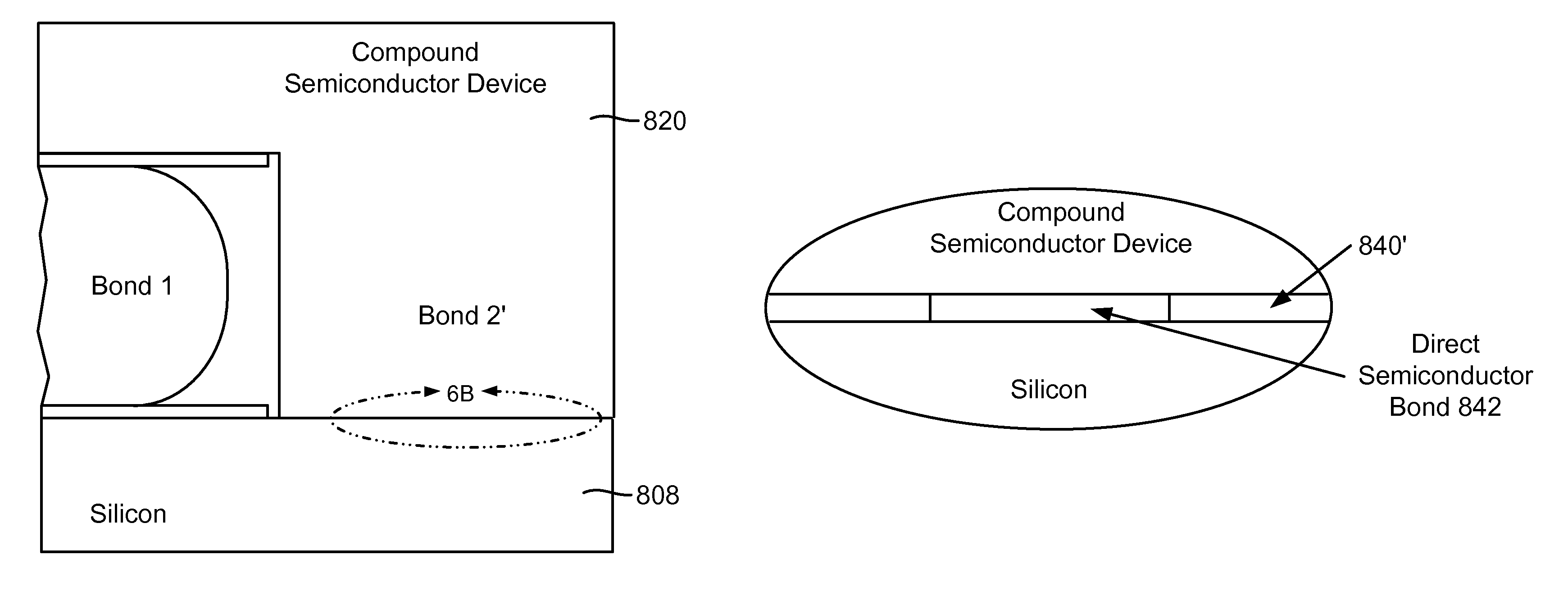
A composite integrated optical device includes a substrate including a silicon layer and a waveguide disposed in the silicon layer. The composite integrated optical device also includes an optical detector bonded to the silicon layer and a bonding region disposed between the silicon layer and the optical detector. The bonding region includes a metal-assisted bond at a first portion of the bonding region. The metal-assisted bond includes an interface layer positioned between the silicon layer and the optical detector. The bonding region also includes a direct semiconductor-semiconductor bond at a second portion of the bonding region.

Description

CROSS-REFERENCES TO RELATED APPLICATIONS[0001]This present application is a continuation-in-part of U.S. patent application Ser. No. 12 / 902,621, filed on Oct. 12, 2010, which claims priority to U.S. Provisional Patent Application No. 61 / 251,132, filed on Oct. 13, 2009, the disclosures of which are hereby incorporated by reference in their entirety for all purposes. U.S. patent application Ser. No. 12 / 902,621 was filed concurrently with 12 / 903,025, the disclosure of which is hereby incorporated by reference in its entirety for all purposes.BACKGROUND OF THE INVENTION[0002]Silicon integrated circuits (“ICs”) have dominated the development of electronics and many technologies based upon silicon processing have been developed over the years. Their continued refinement led to nanoscale feature sizes that can be critical for making complementary metal oxide semiconductor CMOS circuits. On the other hand, silicon is not a direct bandgap materials. Although direct bandgap materials, includi...

Claims


Application Information

Patent Timeline
Patent Type & Authority Patents(United States)
IPC IPC(8): H01S5/00
CPCG02B6/12G02B6/4245G02B6/4232H01S5/021H01S5/02272H01L2224/73259H01L2224/24H01S5/0237
Inventor KRASULICK, STEPHEN B.DALLESASSE, JOHN
Owner SKORPIOS TECH
Learn More