Semiconductor device and method of manufacturing the same

a semiconductor and semiconductor wafer technology, applied in the direction of semiconductor devices, basic electric elements, electrical equipment, etc., can solve the problems of increasing the diameter the deformation of the turn-off characteristic, and the size of the semiconductor wafer

Active Publication Date: 2013-12-17
SEMICON COMPONENTS IND LLC
View PDF5 Cites 0 Cited by
  • Summary
  • Abstract
  • Description
  • Claims
  • Application Information

AI Technical Summary

Benefits of technology

[0016]Furthermore, the embedded collector layer and so on of the NPN bipolar transistor forming the control circuit or a P type low concentration embedded layer of a high breakdown voltage junction FET used for a level shifter in the P− type semiconductor substrate 51 need be formed in an inner region of the P− type semiconductor substrate 51 at about several μm from the front surface thereof. This need an ion implantation machine that applies a high current and high acceleration energy, and it is necessary to avoid crystal defects when ion implantation is performed. It is also necessary to address problems caused by using this P− type semiconductor substrate 51.

Problems solved by technology

However, on the contrary, this has a problem of increasing the time until the recombination and extinction of excess injected holes are completed when the IGBT turns off, thereby causing degradation in the turn-off characteristic.
However, since the diameters of semiconductor wafers are becoming larger, a Czochralski (CZ) wafer need be used instead of a FZ wafer having difficulty in increasing the diameter.
This causes a problem in increasing the breakdown voltage and decreasing the leakage current.
When a device element such as IGBT is formed on such a P− type semiconductor substrate, there is a problem that a planarization treatment need be performed on the polysilicon film.

Method used


Image

  • Semiconductor device and method of manufacturing the same
  • Semiconductor device and method of manufacturing the same
  • Semiconductor device and method of manufacturing the same

Examples


Embodiment Construction

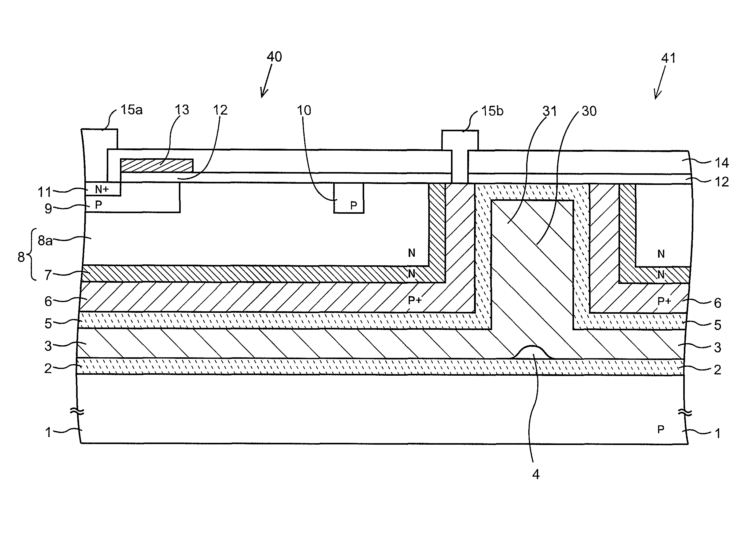
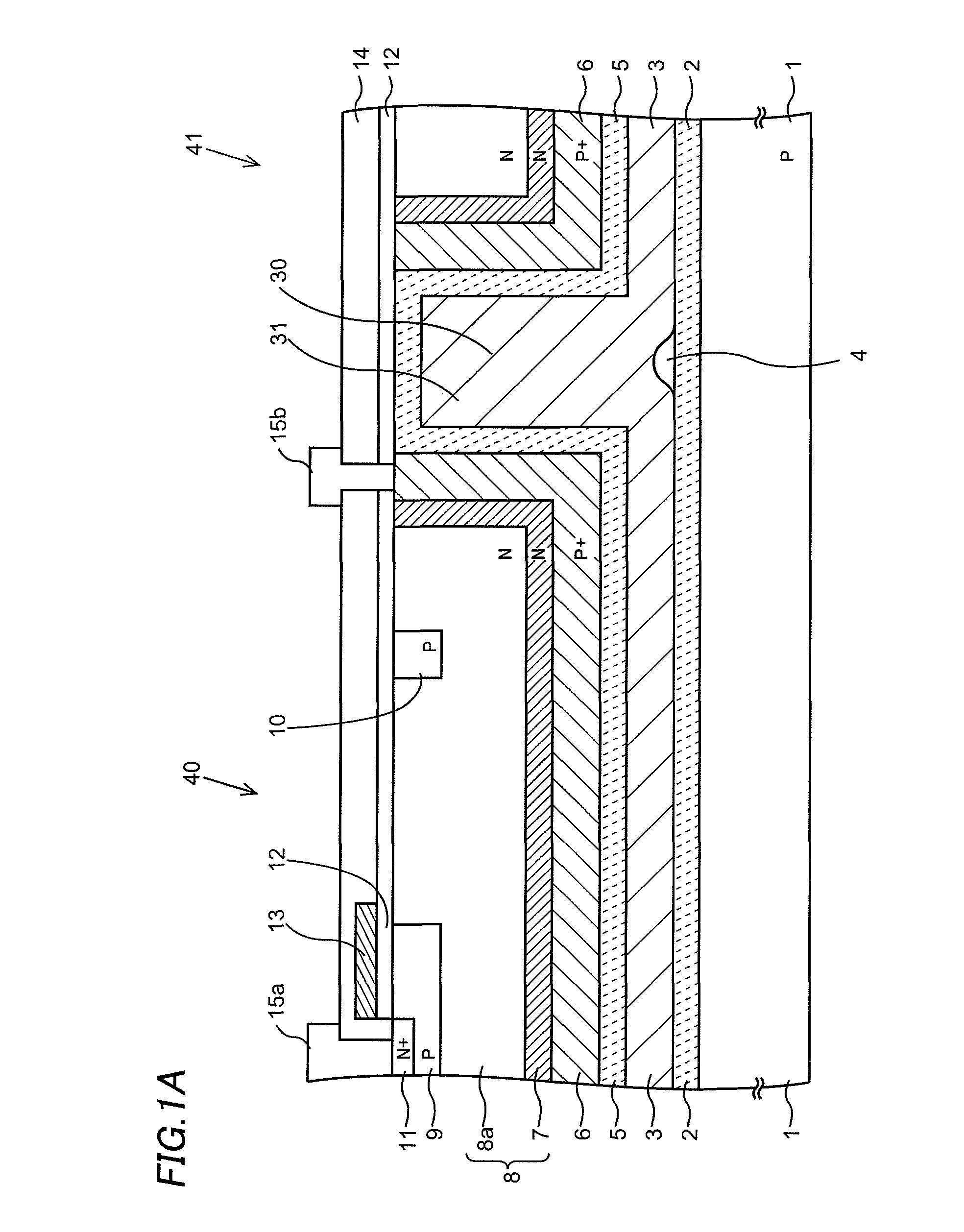
[0027]A first embodiment of the invention will be described referring to FIG. 1. FIG. 1A is a cross-sectional view of a semiconductor device enlargedly showing a trench 30, a region 40 for an IGBT and a region 41 for a control circuit for the IGBT and so on, the regions being isolated by a dielectric isolation layer 31 made of an embedded insulation film 5 and so on. The IGBT region 40 actually has a symmetrical portion on the left side of an emitter electrode 15a in this figure, that is symmetrical to the portion on the right side, forming an SOI island for the IGBT as a whole.

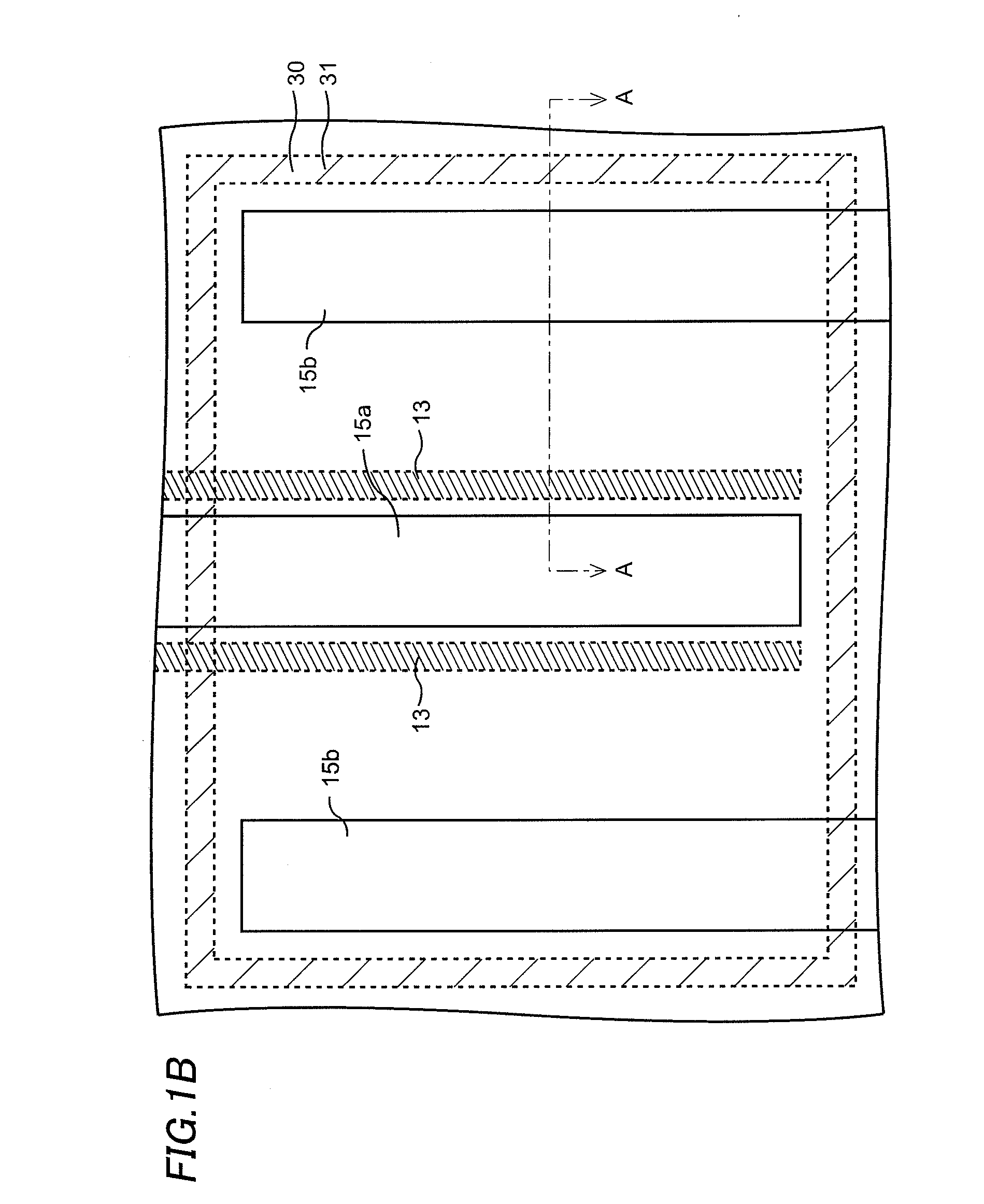
[0028]FIG. 1B is a plan view of the semiconductor device. A plurality of N+ type emitter layers 11 are formed actually so as to increase the channel density although only one of these is shown in the figure. FIG. 1A is the cross-sectional view of FIG. 1B along line A-A.

[0029]The SOI substrate of the IGBT region 40 of the embodiment employs the following structure. A S (Silicon) layer in the SOI layer includes...


PUM


Abstract

In a semiconductor device in which an IGBT, a control circuit for the IGBT and so on are formed on an SOI substrate divided by trenches, the invention is directed to providing the IGBT with a higher breakdown voltage, an enhanced turn-off characteristic and so on. An N type epitaxial layer is formed on a dummy semiconductor substrate, a trench is formed in the N type epitaxial layer, an N type buffer layer and then a P type embedded collector layer are formed on the sidewall of the trench and the front surface of the N type epitaxial layer, and the bottom of the trench and the P+ type embedded collector layer are covered by an embedded insulation film. The embedded insulation film is covered by a polysilicon film, and a P type semiconductor substrate is attached to the polysilicon film with an insulation film being interposed therebetween. Then the dummy semiconductor substrate is removed, thereby forming an SOI substrate having the embedded insulation film, the P+ type embedded collector layer, the N type buffer layer, the N type drift layer and so on that are exposed being almost flush with each other on the bottom of the trench. An IGBT and so on are formed on this SOI substrate.

Description

CROSS-REFERENCE OF THE INVENTION[0001]This application claims priority from Japanese Patent Application No. 2010-125753, the content of which is incorporated herein by reference in its entirety.BACKGROUND OF THE INVENTION[0002]1. Field of the Invention[0003]The invention relates to a semiconductor device that has an IGBT (Insulated Gate Bipolar Transistor) formed on an SOI (Silicon on Insulator) substrate divided by trenches and a method of manufacturing the same.[0004]2. Description of the Related Art[0005]A semiconductor device having an IGBT 54, control and drive circuits 55 for the IGBT 54, and so on formed on an SOI substrate divided by trenches 101,102,103 will be described referring to FIG. 10. A P− type semiconductor substrate 51 on which an IGBT 54, a control circuit 55 and so on are formed and isolated by dielectric isolation layers 56, 57, 58 is attached to a P− type semiconductor substrate 53 that is a supporting substrate and insulated from the P− type semiconductor sub...

Claims


Application Information

Patent Timeline
Patent Type & Authority Patents(United States)
IPC IPC(8): H01L29/739
CPCH01L21/76283H01L21/84H01L29/66325H01L29/7394H01L29/36
Inventor SOMA, MITSURU
Owner SEMICON COMPONENTS IND LLC
Why Eureka
Try Eureka