
Method of making semiconductor optical integrated device by alternately arranging spacers with integrated device arrays

a technology of integrated devices and spacers, which is applied in the direction of semiconductor lasers, nanotechnology, lasers, etc., can solve the problems of mechanically and electrically, difficult to stably fix the plurality of semiconductor optical integrated devices in place, and poor adhesion of bonding wires to the bonding pads, so as to prevent the generation of a gap between the first bonding pad and the spacer, and reduce the flow of coating-film materials to the surface of the bonding pads

Inactive Publication Date: 2013-10-22
SUMITOMO ELECTRIC IND LTD
View PDF118 Cites 2 Cited by
  • Summary
  • Abstract
  • Description
  • Claims
  • Application Information

AI Technical Summary

Benefits of technology

The present invention provides a method for making a semiconductor optical integrated device with a movable spacer that prevents generation of a gap between the bonding pad and the spacer. The movable portion of the spacer can be adjusted to appropriately prevent the gap. The method also includes forming a first dummy pad on a side opposite to the first bonding pad to protect the optical waveguide and maintain parallelism between the spacers and the semiconductor optical integrated device arrays. The first dummy pad can be easily formed without performing an additional step.

Problems solved by technology

As a result, it is difficult to stably fix the plurality of semiconductor optical integrated devices in place.
When the surface of the bonding pad is covered by the coating-film material, a bonding wire adheres poorly to the bonding pad.
So, it is difficult to connect the bonding wire to the bonding pad, mechanically and electrically.

Method used


Image

  • Method of making semiconductor optical integrated device by alternately arranging spacers with integrated device arrays
  • Method of making semiconductor optical integrated device by alternately arranging spacers with integrated device arrays
  • Method of making semiconductor optical integrated device by alternately arranging spacers with integrated device arrays

Examples


Embodiment Construction

[0023]Hereinafter, a method of making a semiconductor optical integrated device according to the present invention will be described in detail with respect to the drawings. In the description, the same elements will be denoted by the same numerals and redundant description will be omitted.

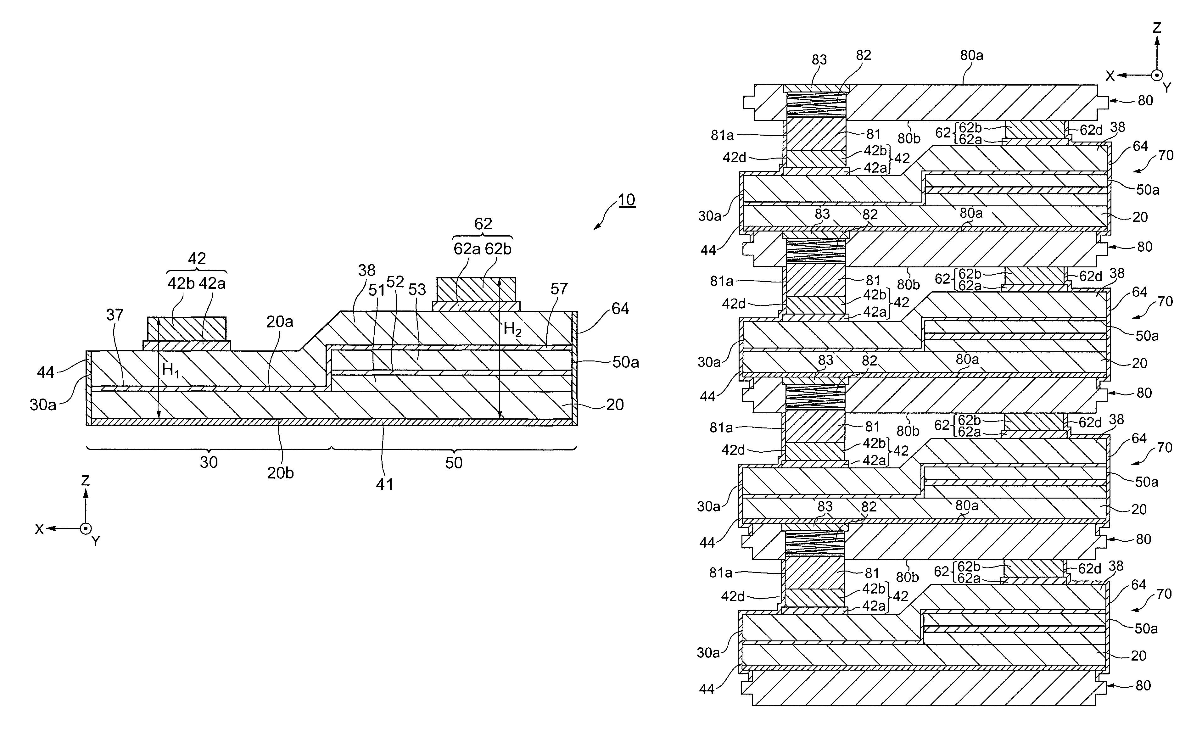
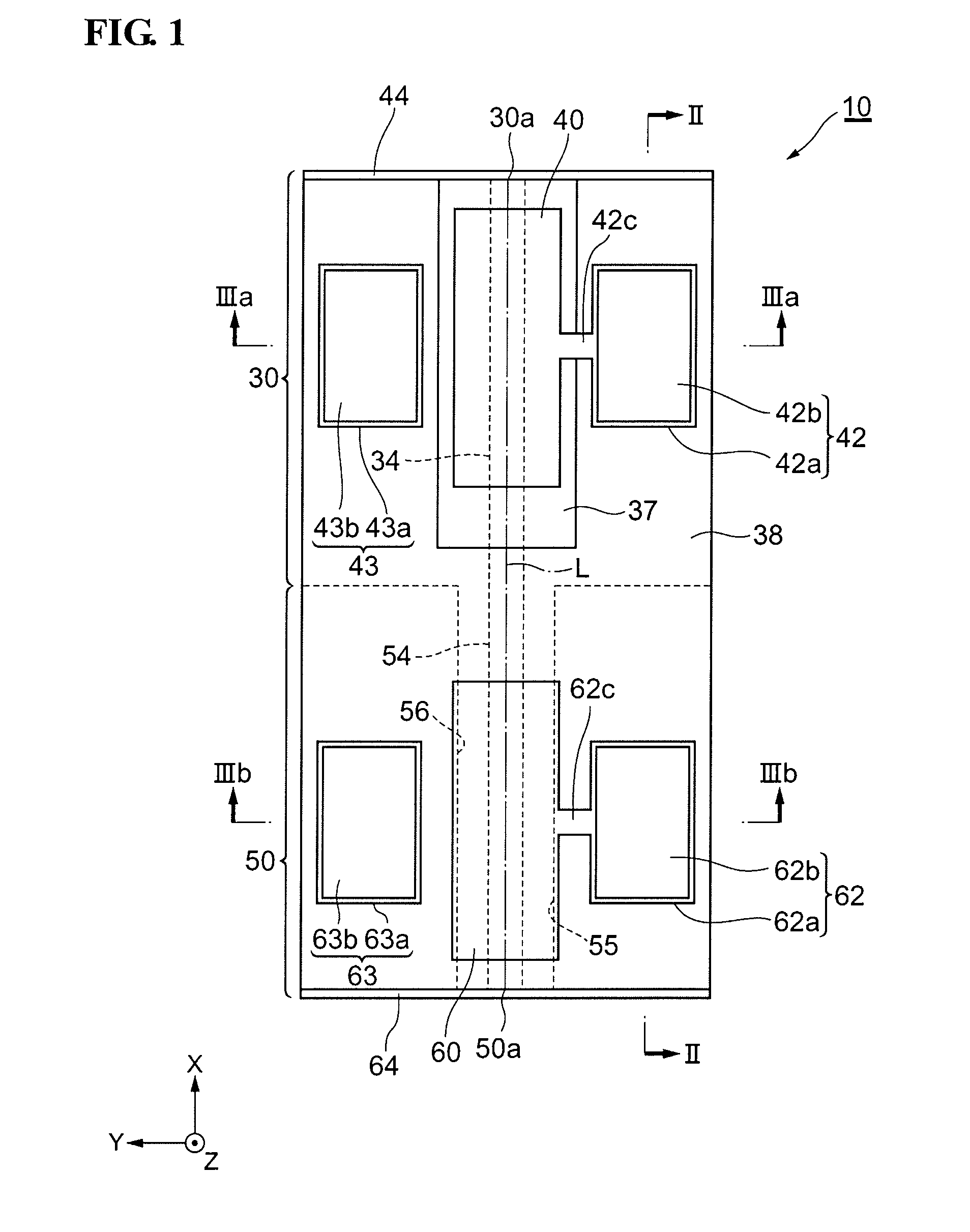
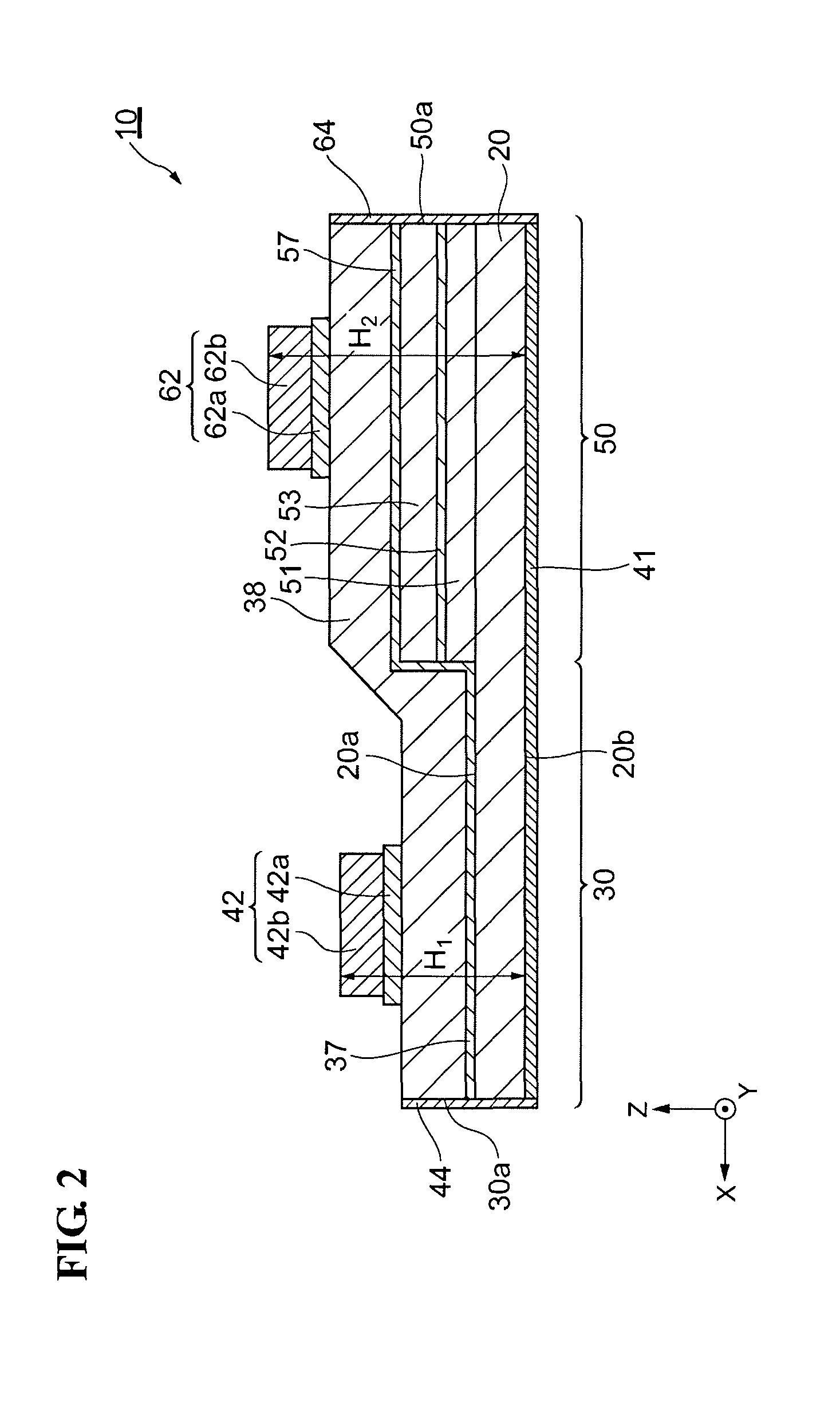
[0024]First, the structure of a semiconductor optical integrated device 10 made by the method according to the present embodiment will be described. The semiconductor optical integrated device 10 is a monolithic integrated semiconductor optical waveguide device that is mainly used in an optical fiber communication system. FIG. 1 is a plan view of the semiconductor optical integrated device 10. FIG. 2 is a sectional view of the semiconductor optical integrated device 10 taken along line II-II of FIG. 1. FIG. 3A is a sectional view of the semiconductor optical integrated device 10 taken along line IIIa-IIIa of FIG. 1. FIG. 3B is a sectional view of the semiconductor optical integrated device 10 taken...


PUM


Abstract

A method of making a semiconductor optical integrated device includes the steps of forming, on a substrate, a plurality of semiconductor integrated devices including a first optical semiconductor element having a first bonding pad and a second optical semiconductor element; forming a plurality of bar-shaped semiconductor optical integrated device arrays by cutting the substrate, each of the semiconductor optical integrated device arrays including two or more semiconductor optical integrated devices; alternately arranging the plurality of semiconductor optical integrated device arrays and a plurality of spacers in a thickness direction of the substrate so as to be fixed in place; and forming a coating film on a facet of the semiconductor optical integrated device array. Furthermore, the spacer has a movable portion facing the first bonding pad, the movable portion protruding toward the first bonding pad and being displaceable in a protruding direction.

Description

BACKGROUND OF THE INVENTION[0001]1. Field of the Invention[0002]The present invention relates to a method of making a semiconductor optical integrated device.[0003]2. Description of the Related Art[0004]To date, semiconductor optical integrated devices having a butt joint structure have been known. For example, Japanese Unexamined Patent Application Publication No. 7-263655 describes a semiconductor optical integrated device including a semiconductor laser and an electro-absorption (EA) modulator. The semiconductor laser and the electro-absorption (EA) modulator are optically coupled to each other through a butt joint and integrated with each other on a single substrate.SUMMARY OF THE INVENTION[0005]A semiconductor optical integrated device includes a first optical semiconductor element that is, for example, a semiconductor laser; and a second optical semiconductor element that is, for example, an optical modulator. The first and second optical semiconductor elements are monolithica...

Claims


Application Information

Patent Timeline
Patent Type & Authority Patents(United States)
IPC IPC(8): H01L21/00
CPCH01S5/02272H01S5/0265H01S5/028B82Y20/00H01S5/0201H01S5/0202H01S5/02264H01S5/0425H01S5/2275H01S5/34306H01S5/2224H01S2301/176H01S5/04252H01S5/04256H01S5/02365H01S5/0237
Inventor YONEDA, YOSHIHIROKOBAYASHI, HIROHIKOKOYAMA, KENJIYANAGISAWA, MASAKIHIRATSUKA, KENJI
Owner SUMITOMO ELECTRIC IND LTD
Learn More