Compensation circuitry of gate driving pulse signal and display device
a compensation circuit and gate driving technology, applied in the field of display fields, can solve the problems of degrading the reliability of the display panel, excessively large or small voltage difference between the highest-level voltage and the lowest-level voltage of each gate driving pulse signal, and the display panel would have poor display quality, so as to achieve the effect of improving the output of the gate driving circui
- Summary
- Abstract
- Description
- Claims
- Application Information
AI Technical Summary
Benefits of technology
Problems solved by technology
Method used
Image

Examples
Embodiment Construction
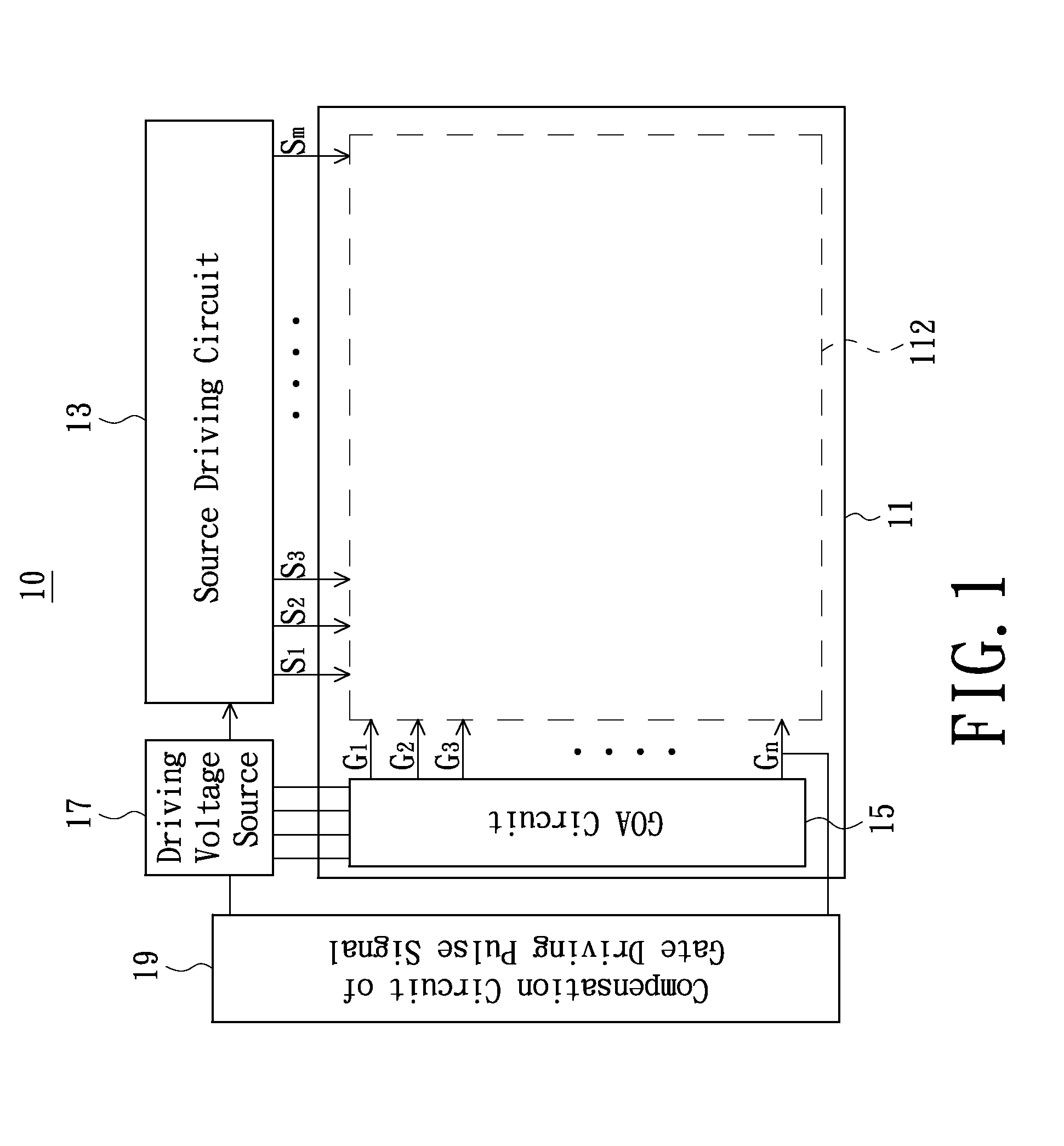
[0006]The present invention is directed to a compensation circuitry of gate driving pulse signal, for effectively improving the output of gate driving circuit.
[0007]The present invention is further directed to a display device, which can solve the issue of poor display quality or being unable to normally startup associated with a display panel by improving the output of gate driving circuit.
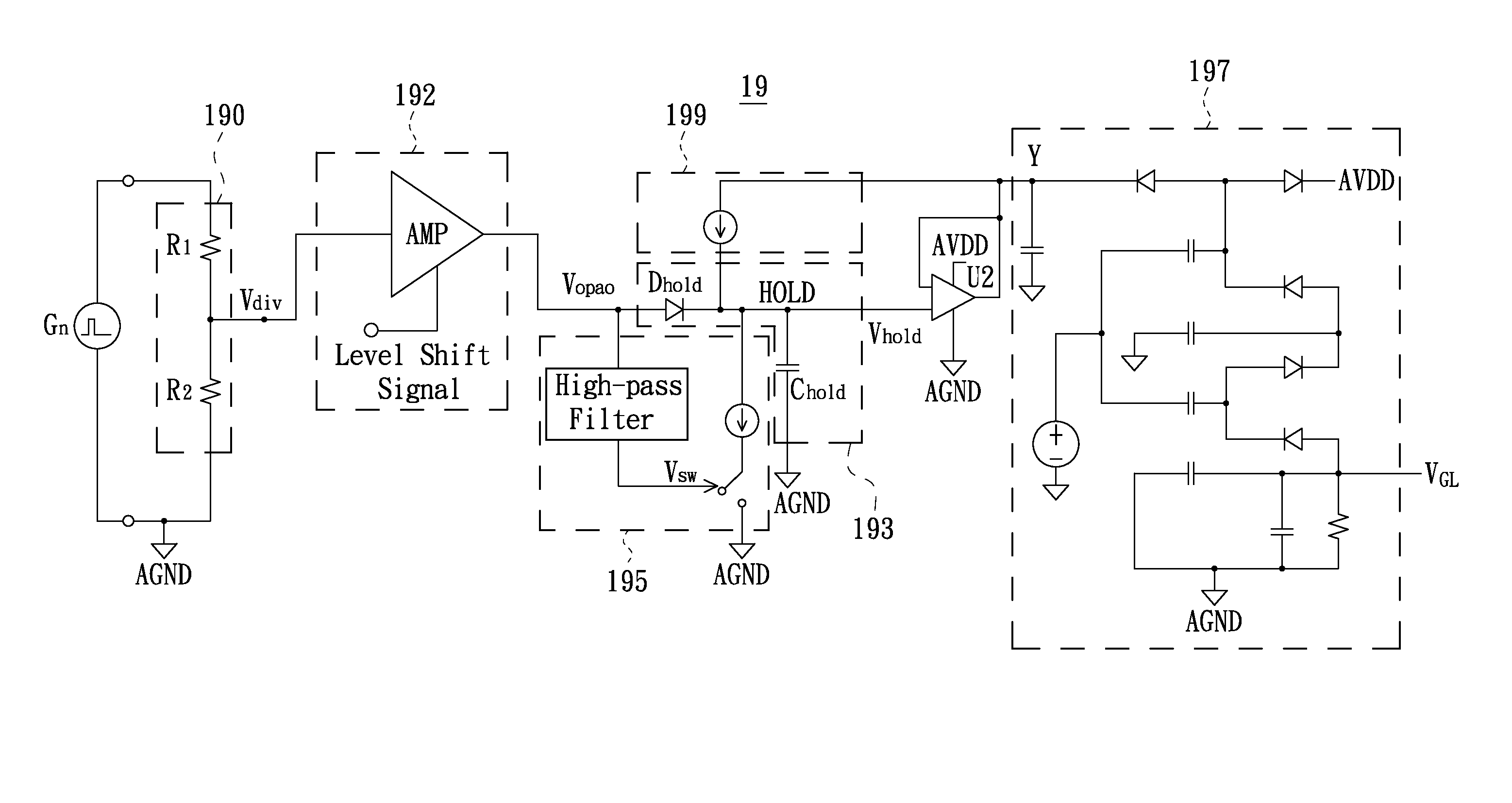
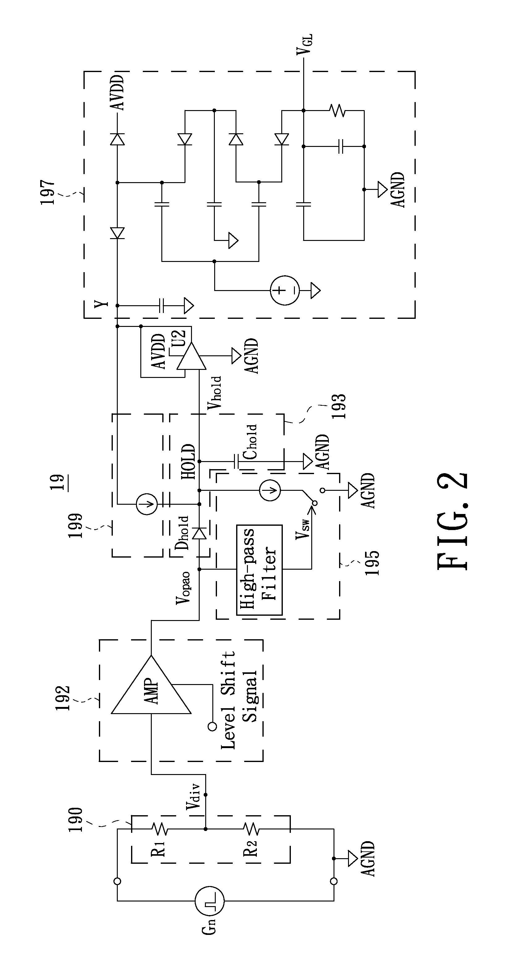
[0008]More specifically, a compensation circuitry of gate driving pulse signal in accordance with an embodiment of the present invention is adapted for receiving a gate driving pulse signal generated from a gate driving circuit in a frequency period. The compensation circuitry includes a pre-processing circuit, a peak detector, a discharge circuit, a voltage buffer and a charge pump circuit. The pre-preprocessing circuit performs a pre-processing operation to the gate driving pulse signal to adjust a voltage of the gate driving pulse signal. The peak detector receives the pre-processed gate drivi...
PUM
 Abstract
Description
Claims
Application Information
 - R&D
- Intellectual Property
- Life Sciences
- Materials
- Tech Scout
- Unparalleled Data Quality
- Higher Quality Content
- 60% Fewer Hallucinations
Browse by: Latest US Patents, China's latest patents, Technical Efficacy Thesaurus, Application Domain, Technology Topic, Popular Technical Reports.
© 2025 PatSnap. All rights reserved.Legal|Privacy policy|Modern Slavery Act Transparency Statement|Sitemap|About US| Contact US: help@patsnap.com