Device and method for supporting a substrate

a technology of substrate and support device, which is applied in the direction of metal-working machine components, metal working apparatus, manufacturing tools, etc., can solve the problems of abnormal transfer of substrate between the stage and the substrate transport device, abnormal processing of the substrate, etc., to enhance the wear resistance of the substrate mount, and improve the strength of the substrate mount

Active Publication Date: 2013-09-10
TOKYO ELECTRON LTD
View PDF31 Cites 135 Cited by
  • Summary
  • Abstract
  • Description
  • Claims
  • Application Information

AI Technical Summary

Benefits of technology

[0015]The present invention has been made under the above circumstances, and an object of the invention is to provide a device and method adapted to prevent abnormal supporting of a substrate, caused by wear due to contact with the substrate or by chemical erosion via the substrate due to use of a chemical liquid.
[0016]A first aspect of the present invention is a substrate support device comprising: a support member having a lower-surface support section to support a lower surface of a substrate; and a position restriction section provided on the lower-surface support section, the position restriction section being formed to surround a periphery of the substrate supported on the lower-surface support section and restrict a position of the substrate. At least one of the lower-surface support section and the position restriction section includes a base material and a protective film formed to cover the base material and prevent at least one of wear and chemical erosion to which the base material will be subject.

Problems solved by technology

This failure could in turn lead to a fall of the wafer W from the wafer transport section 101 during carriage or result in abnormal processing of the wafer W due to possible transfer to the improper position in the required module.
These events could cause the wafer W to be mounted or inclined in positionally shifted form with respect to the mounting region on the stage, and result in abnormal processing of the wafer W or in abnormal transfer thereof between the stage and the substrate transport device.
In Japanese Patent No. 3355950 (Paragraph 0017), although using a diamond-like carbon film to cover the surface of a resin-formed base for a machine part is described, problems associated with carriage and mounting of the substrate as discussed above are not described and thus the problems cannot be solved.

Method used


Image

  • Device and method for supporting a substrate
  • Device and method for supporting a substrate
  • Device and method for supporting a substrate

Examples


first embodiment

[0098]A first embodiment of the present invention will be described using FIGS. 1 to 18.

[0099]A coating / developing apparatus 1 with a substrate transport device of the present invention is first described below.

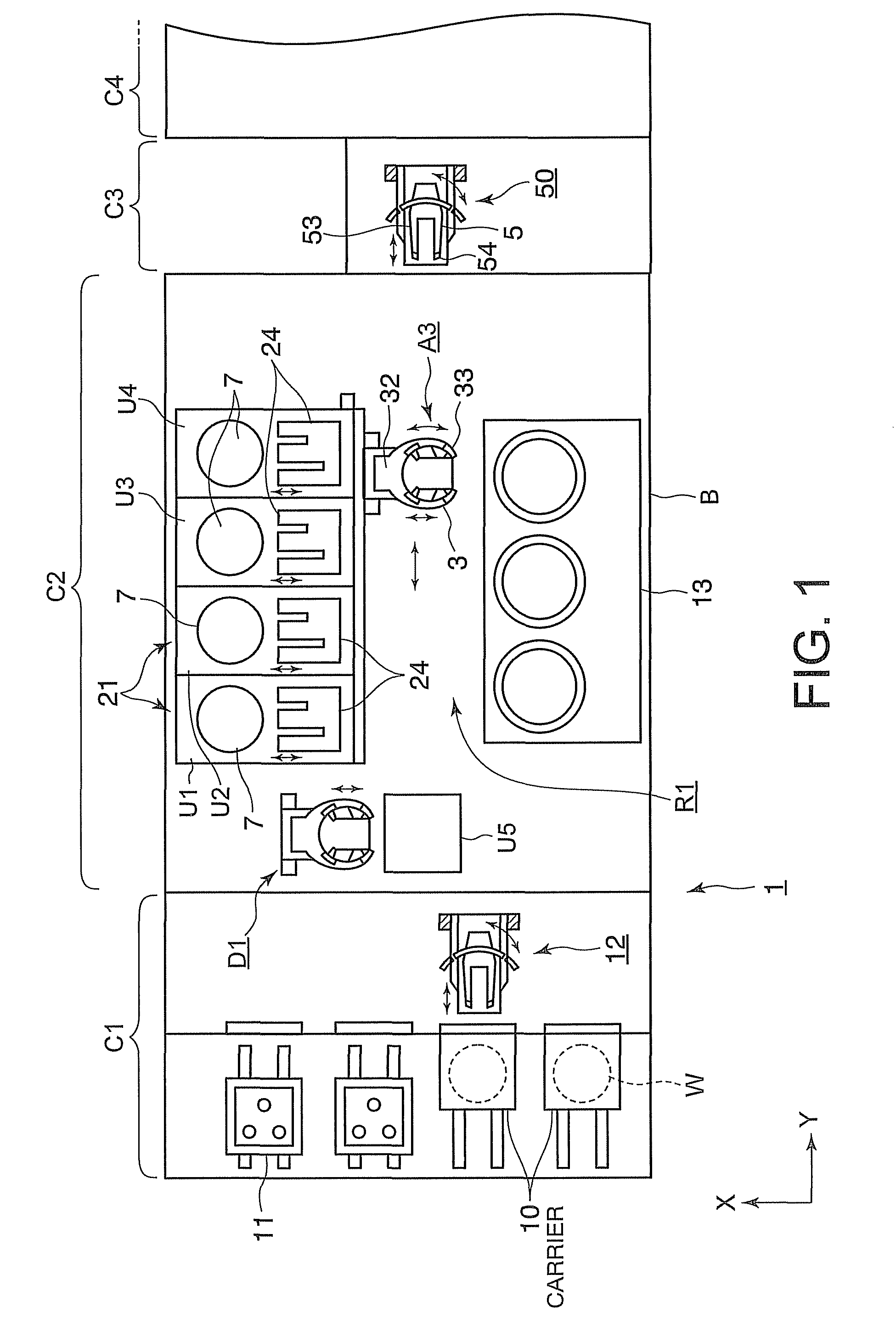
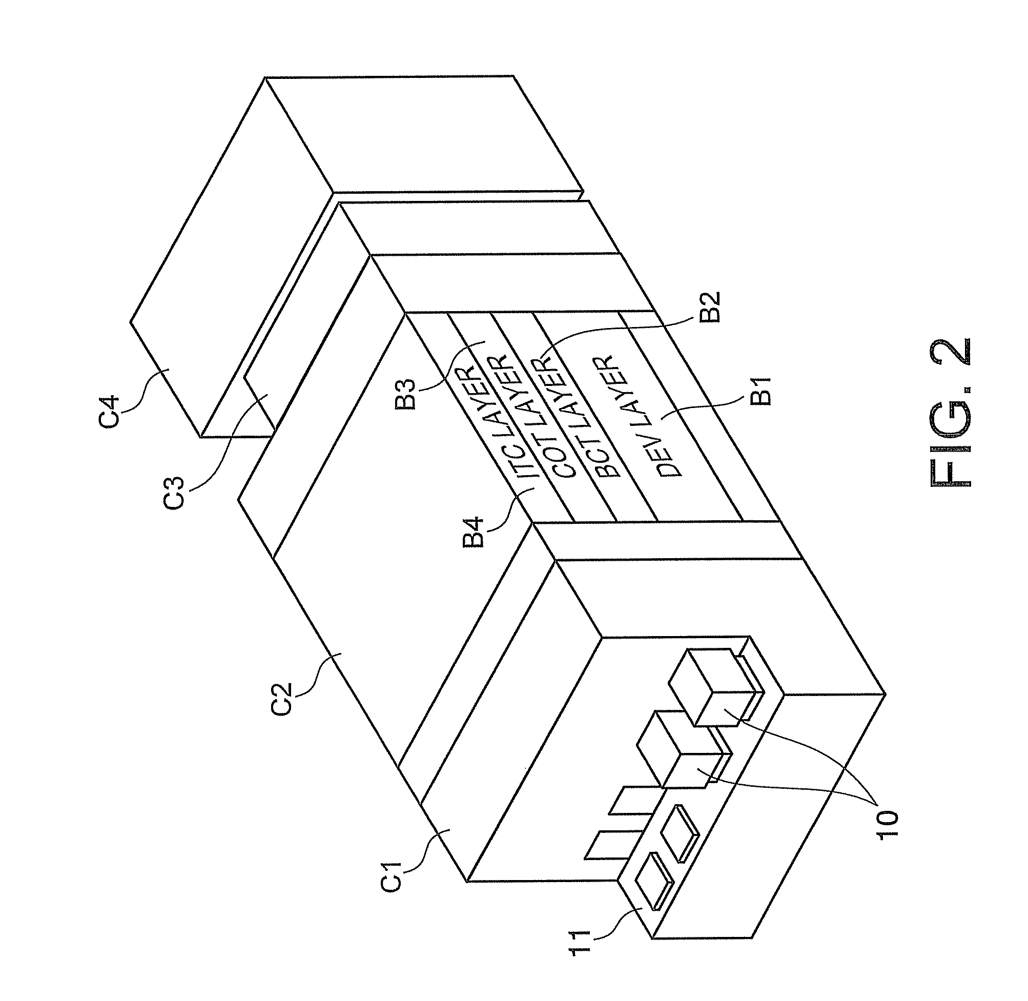
[0100]FIG. 1 is a plan view of a resist pattern forming system including an exposure apparatus C4 connected to the coating / developing apparatus 1. FIG. 2 is a perspective view of the system. FIG. 3 is a longitudinal, sectional side view of the system. The coating / developing apparatus 1 includes a carrier block C1. The carrier block C1 is constructed so that a transfer arm 12, after unloading a wafer W from an enclosed type of carrier 10 mounted on a mounting table 11 of the carrier block C1, transfers the wafer W to a processing block C2, then receives a processed wafer W from the processing block C2, and returns the wafer W to the carrier 10.

[0101]As shown by way of example in FIG. 3, the processing block C2 includes a first block (DEV layer) B1 for a developing process, a s...

second embodiment

[0168]Next, a second embodiment of the present invention will be described referring to FIGS. 21 to 30.

[0169]In the second embodiment of FIGS. 21 to 30, the same sections as those of the first embodiment shown in FIGS. 1 to 18 are each assigned the same reference number or symbol, and detailed description of the same sections is omitted.

[0170]As shown in FIGS. 21 and 22(b), a protective film 41 is formed, in two-layered form on the surfaces of the lower-surface support section 34, the lower vertical wall 35, and the inclined section 36. The protective film 41 includes a lower layer 42 and an upper layer 43, each of which is made of diamond-like carbon (DLC), an amorphous hard film made of a hydrocarbon or of an allotrope of carbon. Reference number 44 in FIG. 22(b) denotes through-holes (through-defects) formed in the layers 42 and 43 during film deposition. Compared with the base material 40, the DLC has high hardness and hence, high resistance to wear. In addition, the DLC has hig...

third embodiment

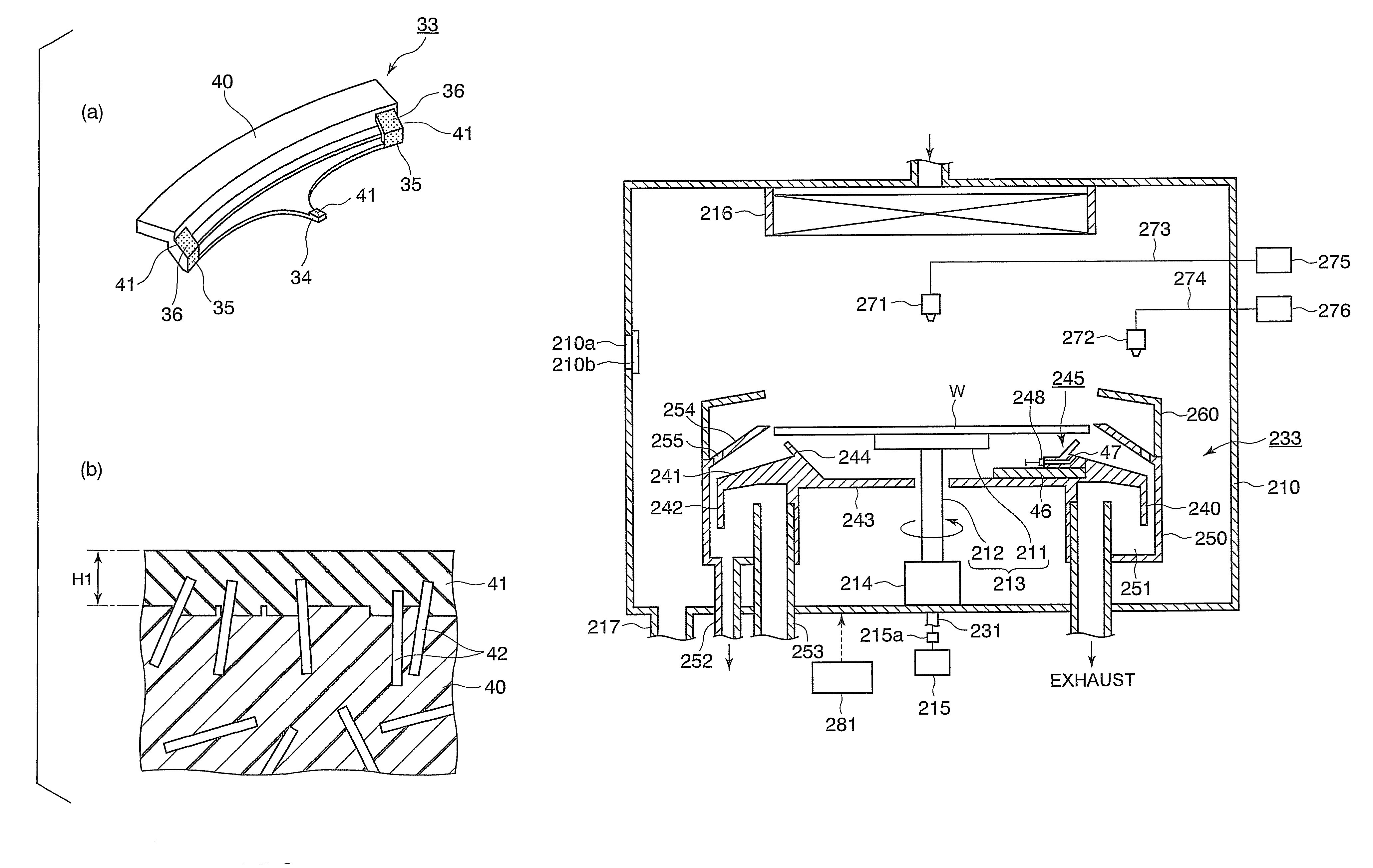
[0222]Next, a third embodiment of the present invention is described below referring to FIGS. 31 to 44.

[0223]An embodiment in which a chemical processing apparatus according to the present invention is applied to a resist coater is described. As shown in FIG. 31, the resist coater includes the following: a spin chuck (vacuum chuck) 213 including a substantially disc-shaped table 211 that is a substrate mount for retaining horizontally a substrate, for example, a semiconductor wafer W (hereinafter, referred to simply as the wafer W) by vacuum-attracting the wafer W from its lower surface, and a rotating shaft 212 connected centrally to a lower face of the table 211; and a resist nozzle 271 that is a process liquid supply element for supplying a process liquid, for example, a resist liquid, to the wafer W.

[0224]A rotary drive 214 that supports the rotating shaft 212 both rotatably about a vertical axis and liftably is connected to a lower end of the rotating shaft 212. Reference numbe...


PUM

PropertyMeasurementUnit
sizesaaaaaaaaaa
sizesaaaaaaaaaa
temperatureaaaaaaaaaa

Abstract

A substrate support device including a support member having a lower-surface support section to support a lower surface of a substrate; and a position restriction section provided on the lower-surface support section, the position restriction section being formed to surround a periphery of the substrate supported on the lower-surface support section and restrict a position of the substrate. At least one of the lower-surface support section and the position restriction section includes a base material and a protective film formed to cover the base material and prevent at least one of wear and chemical erosion to which the base material will be subject. The substrate support device further includes, for example, a base that supports the support member, and a driving structure that moves the support member in a relative fashion with respect to the base, and is constructed as a substrate transport device.

Description

BACKGROUND OF THE INVENTION[0001]1. Field of the Invention[0002]The present invention relates to a device and method for supporting a substrate.[0003]2. Description of the Related Art[0004]During a photoresist process that is one of semiconductor-manufacturing processes, a resist pattern is formed on semiconductor wafers (hereinafter, referred to simply as wafers) by coating the wafer surface with a resist and exposing the resist to light in the desired pattern, followed by development. Such processing is usually performed using a system that includes a coating / developing apparatus for resist coating / development and an exposure apparatus connected to the coating / developing apparatus.[0005]The coating / developing apparatus includes various modules. These modules are, for example, a resist-coating module for coating each wafer with the resist, a developing module for supplying a developing solution, and a heating or cooling module for heating or cooling the wafer before and / or after pr...

Claims


Application Information

Patent Timeline
Patent Type & Authority Patents(United States)
IPC IPC(8): B23Q3/00B25B1/00
CPCH01L21/67742H01L21/68707Y10T29/53961Y10T29/49998
Inventor NAKANO, SEIJIMATSUSHITA, MICHIAKIIIDA, NARUAKIENOKIDA, SUGURUMORIKAWA, KATSUHIRO
Owner TOKYO ELECTRON LTD
Why Eureka
Try Eureka