Semiconductor device with strain-inducing regions and method thereof

a technology of semiconductors and regions, applied in the direction of semiconductor/solid-state device manufacturing, basic electric elements, electric devices, etc., can solve the problems of reducing manufacturing yield, many practical difficulties in implementing such structures, and integrity problems of gate dielectrics

Active Publication Date: 2013-09-03
GLOBALFOUNDRIES INC
View PDF2 Cites 8 Cited by
  • Summary
  • Abstract
  • Description
  • Claims
  • Application Information

AI Technical Summary

Benefits of technology

[0003]Improved MOSFET devices (60) are obtained by incorporating strain inducing source-drain regions (62, 64) whose closest facing “nose” portions (621, 641) underlying the gate (28) are located at different depths (622, 642) from the device surface (25). In a preferred embodiment, the spaced-apart source-drain regions (62, 64) may laterally overlap (43). This close proximity increases the favorable impact of the strain inducing source-drain regions (62, 64) on the carrier mobility in a channel region (49) between the source and drain (62, 64). The source-drain regions (62, 64) are desirably formed by epitaxially refilling asymmetric cavities (62′, 64′) etched from both sidewalls (271′, 272′) of the gate (28). Cavity asymmetry is obtained by forming an initial cavity (74) proximate only one sidewall (272′) of the gate (28) and then etching the final spaced-apart source-drain cavities (62′, 64′) proximate both sidewalls (271′, 272′) of the gate (28) along predetermined crystallographic directions. The finished cavities (62′, 64′) having different depths (625′, 645′) and nose regions (621′, 641′) at different heights extending toward each other under the gate (28), are epitaxially refilled with the strain inducing semiconductor material for the source-drain regions (62, 64).

Problems solved by technology

However, many practical difficulties are encountered in implementing such structures.
For example, and not intended to be limiting, bringing the strain inducing source-drain regions closer to the gate edges in order to enhance the localized strain beneath the gate often leads to integrity problems with the gate dielectric and reduced manufacturing yield.

Method used


Image

  • Semiconductor device with strain-inducing regions and method thereof
  • Semiconductor device with strain-inducing regions and method thereof
  • Semiconductor device with strain-inducing regions and method thereof

Examples


Embodiment Construction

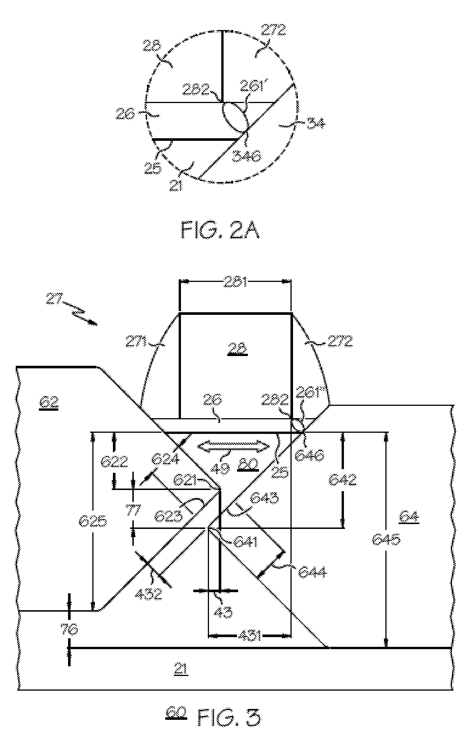
[0011]The following detailed description is merely exemplary in nature and is not intended to limit the invention or the application and uses of the invention. Furthermore, there is no intention to be bound by any expressed or implied theory presented in the preceding technical field, background, or the following detailed description. For simplicity and clarity of illustration, the drawing figures illustrate the general manner of construction, and descriptions and details of well-known features and techniques may be omitted to avoid unnecessarily obscuring the invention. Additionally, elements in the drawings figures are not necessarily drawn to scale. For example, the dimensions of some of the elements or regions in the figures may be exaggerated relative to other elements or regions to help improve understanding of embodiments of the invention.

[0012]The terms “comprise,”“include,”“have” and any variations thereof, are intended to cover non-exclusive inclusions, such that a process...


PUM


Abstract

Improved MOSFET devices are obtained by incorporating strain inducing source-drain regions whose closest facing “nose” portions underlying the gate are located at different depths from the device surface. In a preferred embodiment, the spaced-apart source-drain regions may laterally overlap. This close proximity increases the favorable impact of the strain inducing source-drain regions on the carrier mobility in an induced channel region between the source and drain. The source-drain regions are formed by epitaxially refilling asymmetric cavities etched from both sides of the gate. Cavity asymmetry is obtained by forming an initial cavity proximate only one sidewall of the gate and then etching the final spaced-apart source-drain cavities proximate both sidewalls of the gate along predetermined crystallographic directions. The finished cavities having different depths and nose regions at different heights extending toward each other under the gate, are epitaxially refilled with the strain inducing semiconductor material for the source-drain regions.

Description

FIELD OF THE INVENTION[0001]This invention relates generally to structures and methods for forming semiconductor devices, especially field effect transistors (FETs) having strain inducing regions.BACKGROUND OF THE INVENTION[0002]It is known that introduction of strain in semiconductor devices can enhance carrier mobility and therefore enhance drive current capability of such devices. For example, and not intended to be limiting, with silicon semiconductor based metal-oxide-semiconductor (MOS) field effect transistors (FETs) it is known that use of source-drain regions formed of a silicon-germanium (Si—Ge) alloy or mixture can provide compressive strain in the channel region located between the source and drain of PMOS devices. This strain can increase carrier mobility in the channel region and significantly improve overall device properties. However, many practical difficulties are encountered in implementing such structures. For example, and not intended to be limiting, bringing th...

Claims


Application Information

Patent Timeline
Patent Type & Authority Patents(United States)
IPC IPC(8): H01L21/336
CPCH01L29/1608H01L29/78H01L29/7848H01L29/165H01L29/66636H01L29/66659H01L21/26586
Inventor FLACHOWSKY, STEFANHOENTSCHEL, JANSCHEIPER, THILO
Owner GLOBALFOUNDRIES INC
Why Eureka
Try Eureka