Method of manufacturing semiconductor device having a bumped wafer and protective layer

a manufacturing method and semiconductor technology, applied in semiconductor devices, semiconductor/solid-state device details, electrical devices, etc., can solve the problems of increasing the number of steps in such a method, and the generation of cracks cannot be sufficiently reduced, so as to prevent cracks and suppress the increase of the number of steps

Inactive Publication Date: 2013-08-27
NITTO DENKO CORP
View PDF13 Cites 0 Cited by
  • Summary
  • Abstract
  • Description
  • Claims
  • Application Information

AI Technical Summary

Benefits of technology

[0008]The present invention has been made in view of the above-described problems, and an object thereof is to provide a method of manufacturing a semiconductor device that is capable of preventing cracks in the low dielectric materials layer while suppressing an increase in the number of steps.
[0009]The present inventors made investigations to solve these problems associated with conventional approaches. As a result, they found that cracks in the low dielectric material layer can be prevented while suppressing an increase in the number of steps by forming a protective layer on a low dielectric material layer of a bumped wafer, and dicing the bumped wafer and the protective layer together, in accordance with the present invention.
[0011]According to the above-described configuration, the low dielectric material layer is reinforced by the protective layer because the protective layer is formed on the low dielectric material layer of the bumped wafer. After that, the bumped wafer is diced together with the protective layer. As a result, the low dielectric material layer is diced while reinforced by the protective layer, and therefore the generation of cracks in the low dielectric material layer can be suppressed. Because the low dielectric material layer is diced while reinforced by the protective layer, the low dielectric material layer does not have to be removed in advance by laser scribing or the like. As a result, an increase in the number of steps can be suppressed.
[0012]According to the above-described configuration, the melt viscosity of the thermosetting resin layer is preferably 1×10² Pa·S or more and 2×10⁴ Pa·S or less at the temperature when the film for forming a protective layer is pasted onto the bumped wafer, and the shear modulus of the adhesive layer is preferably 3×10⁴ Pa or more and 2×10⁶ Pa or less at the temperature when the film for forming a protective layer is pasted onto the bumped wafer. When the melt viscosity of the thermosetting resin layer is 1×10² Pa·S or more and 2×10⁴ Pa·S or less at the temperature when the film for forming a protective layer is pasted onto the bumped wafer, and the shear modulus of the adhesive layer is 3×10⁴ Pa or more and 2×10⁶ Pa or less at the temperature when the film for forming a protective layer is pasted onto the bumped wafer, the bump can be made to protrude from the thermosetting resin layer when the film for forming a protective layer is pasted onto the bumped wafer. As a result, deterioration of connection reliability can be suppressed.
[0013]Because the melt viscosity of the thermosetting resin layer is 1×10² Pa·S or more at the temperature when the film for forming a protective layer is pasted onto the bumped wafer, the thermosetting resin layer can be prevented from being washed away when the film for forming a protective layer is pasted onto the bumped wafer, and the protective layer can be more certainly formed. Because the melt viscosity of the thermosetting resin layer is less than 2×10⁴ Pa·S at the temperature when the film for forming a protective layer is pasted onto the bumped wafer, the bump can be made to more certainly protrude from the thermosetting resin layer.
[0015]According to the present invention, a method of manufacturing a semiconductor device can be provided that is capable of preventing cracks in a low dielectric material layer while suppressing an increase of the number of steps.

Problems solved by technology

There has been a problem with dicing in that the number of steps increases in such a method because the laser scribing is performed first, followed by dicing with a blade or the like.
Even when the laser scribing is used, the method has room for improvement in that it cannot sufficiently reduce the generation of cracks because the low dielectric material layer is brittle.

Method used


Image

  • Method of manufacturing semiconductor device having a bumped wafer and protective layer
  • Method of manufacturing semiconductor device having a bumped wafer and protective layer
  • Method of manufacturing semiconductor device having a bumped wafer and protective layer

Examples


Embodiment Construction

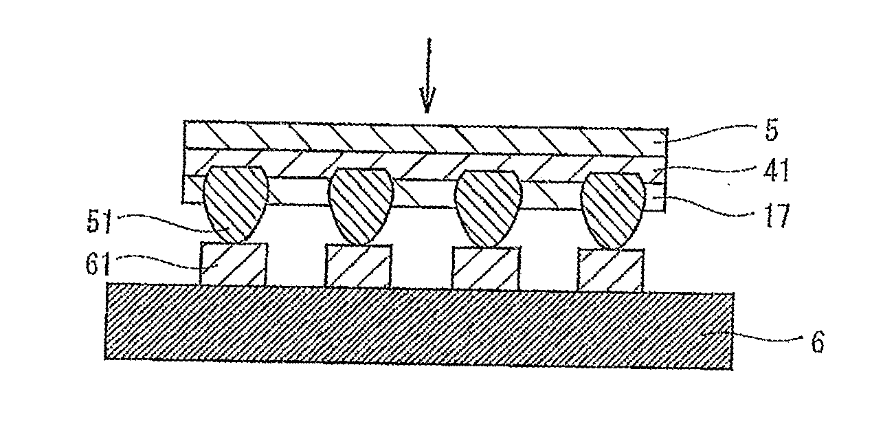
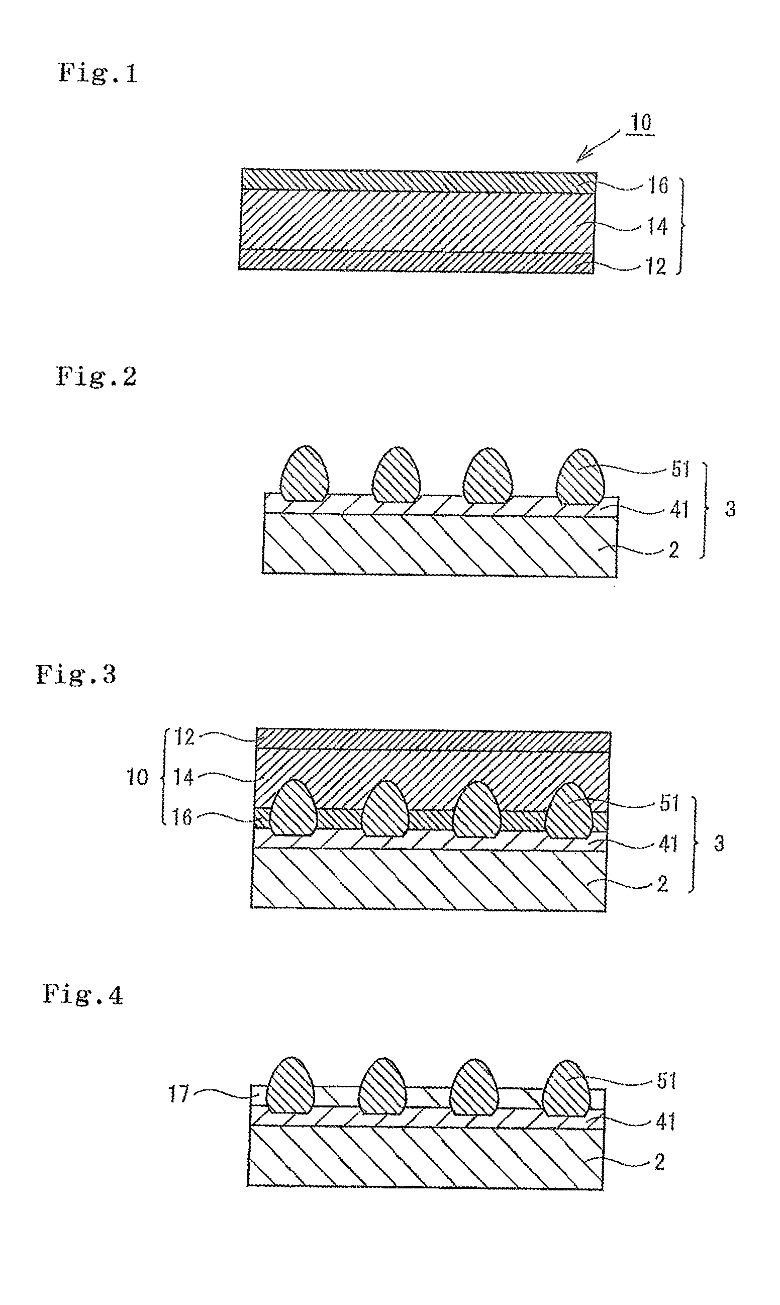
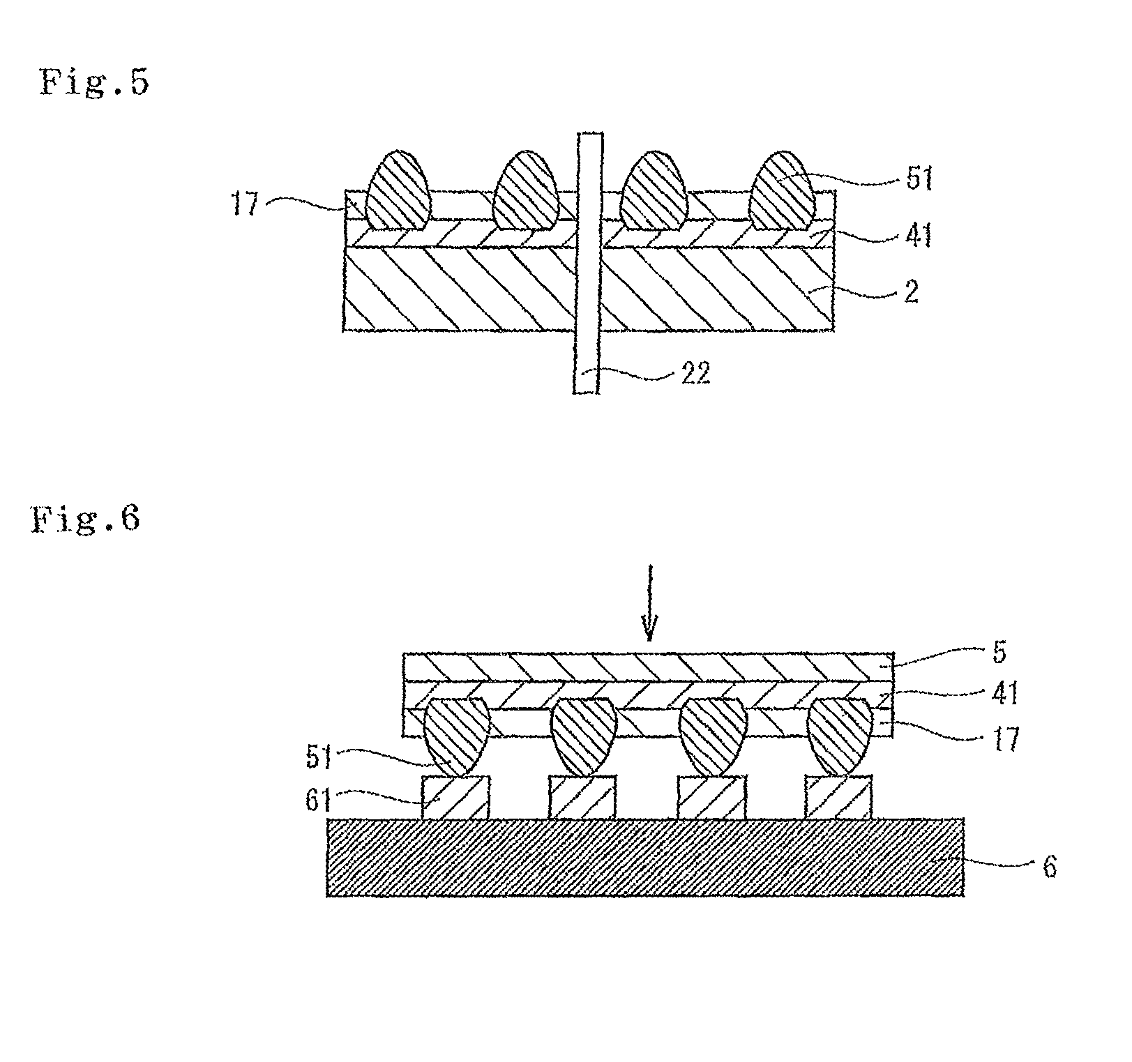
[0034]An embodiment of the present invention is explained by referring to the drawings. However, the present invention is not limited to these examples. Parts in the drawings that are not necessary for the explanation are omitted, and there may be parts that are shown in magnified or reduced scale to facilitate explanation. First, the film for forming a protective layer according to the present embodiment is explained below. FIG. 1 is a sectional view schematically showing one example of the film for forming a protective layer according to the present embodiment.

Film for Forming Protective Layer

[0035]As shown in FIG. 1, a film 10 for forming a protective layer has a configuration in which a support base 12, an adhesive layer 14, and a thermosetting resin layer 16 are laminated, in this order. The surface of the thermosetting resin layer 16 may be protected by a separator or the like until it is pasted onto a wafer.

[0036]A bumped wafer, to which the film 10 for forming a protective l...


PUM

PropertyMeasurementUnit
shear modulusaaaaaaaaaa

Abstract

A method of manufacturing a semiconductor device is provided. The method includes the steps of pasting a film for forming a protective layer in which a support base, an adhesive layer, and a thermosetting resin layer are laminated, in that order, onto a bumped wafer in which a low dielectric material layer is formed, with the thermosetting resin layer serving as a pasting surface, and further, peeling the support base and the adhesive layer from the thermosetting resin layer, forming a protective layer by thermally curing the thermosetting resin layer, and dicing the bumped wafer and the protective layer together.

Description

BACKGROUND OF THE INVENTION[0001]1. Field of the Invention[0002]The present invention relates to a method of manufacturing a semiconductor device using a film for forming a protective layer in which a support base, an adhesive layer, and a thermosetting resin layer are laminated, in this order.[0003]2. Description of Related Art[0004]Conventionally, because the distance between circuits is becoming shorter as the circuit pattern formed on a semiconductor chip is becoming finer, the capacitance between adjacent circuits is becoming greater. A phenomenon occurs according to which a signal traveling in the circuit becomes slow (signal delay) in proportion to the increase in capacitance. It has been proposed to lower the capacitance between circuits by forming a low dielectric material layer on the circuit using a material having a low dielectric constant, a so-called low-k material (low dielectric material).[0005]Examples of the low dielectric material layer include a SiO2 film (relati...

Claims


Application Information

Patent Timeline
Patent Type & Authority Patents(United States)
IPC IPC(8): H01L21/00
CPCH01L21/568H01L23/3157H01L24/10H01L21/6836H01L23/293H01L2221/68377H01L24/81H01L2221/68327H01L2221/6834H01L2221/68363H01L2224/10126H01L2224/16227H01L2224/81191H01L2924/01013H01L2924/01029H01L2924/0103H01L2924/01051H01L2924/01056H01L2924/01079H01L2924/01082H01L2924/01005H01L2924/01006H01L2924/01019H01L2924/0102H01L2924/01024H01L2924/01033H01L2924/01047H01L2924/014H01L2224/16225H01L2924/15787H01L2924/351H01L2924/00H01L21/30
Inventor ODA, TAKASHITAKAMOTO, NAOHIDEMATSUMURA, TAKESHI
Owner NITTO DENKO CORP
Why Eureka
Try Eureka