
Method of depositing film with tailored comformality

a film and comformality technology, applied in the direction of chemical vapor deposition coating, coating, plasma technique, etc., can solve the problems of increasing production cost, increasing processing steps and processing complexity, and difficult to form pre-patterned features with flat tops, so as to prevent damage to the underlying, fine and precise control

Active Publication Date: 2013-06-25
ASM JAPAN
View PDF4 Cites 380 Cited by
  • Summary
  • Abstract
  • Description
  • Claims
  • Application Information

AI Technical Summary

Benefits of technology

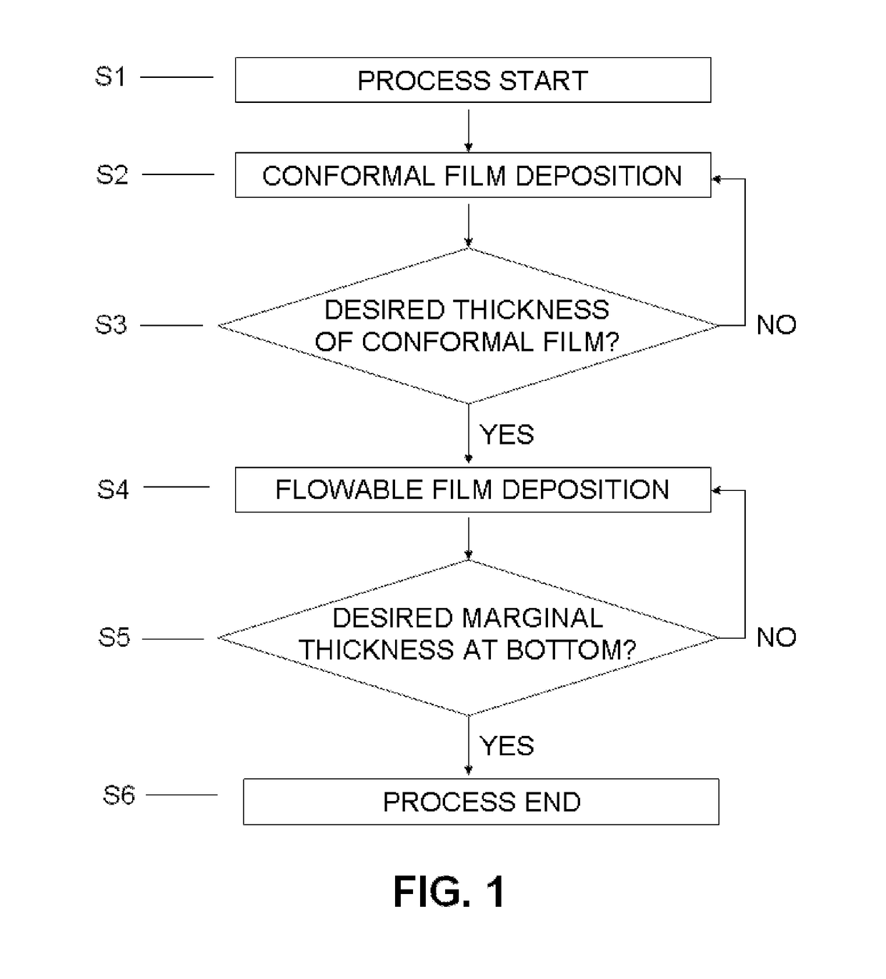
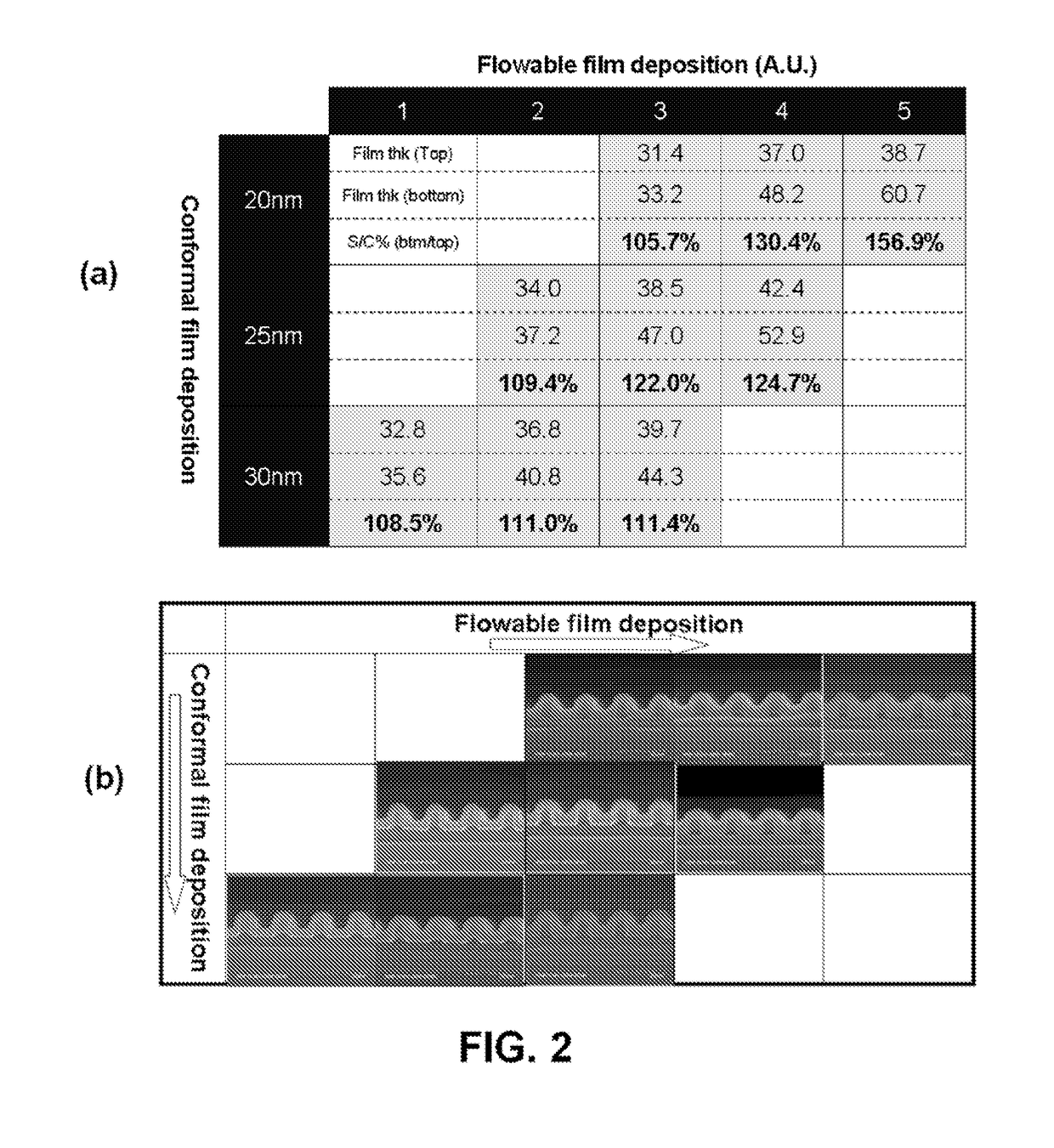
The patent text describes a method of depositing a film with different thicknesses at different locations, such as top, bottom, and sides. The method combines conformal film deposition and flowable film deposition. This method allows for precise control over the film thickness and ensures uniform thickness across multiple walls. The technique can be used in various applications, such as Spacer, Sacrificial Layer, and others. The technical effect is the solution of the residual spacer problem without any additional hardmask layer and the simultaneous control over the thickness of films depositing on side walls and top / bottom surfaces.

Problems solved by technology

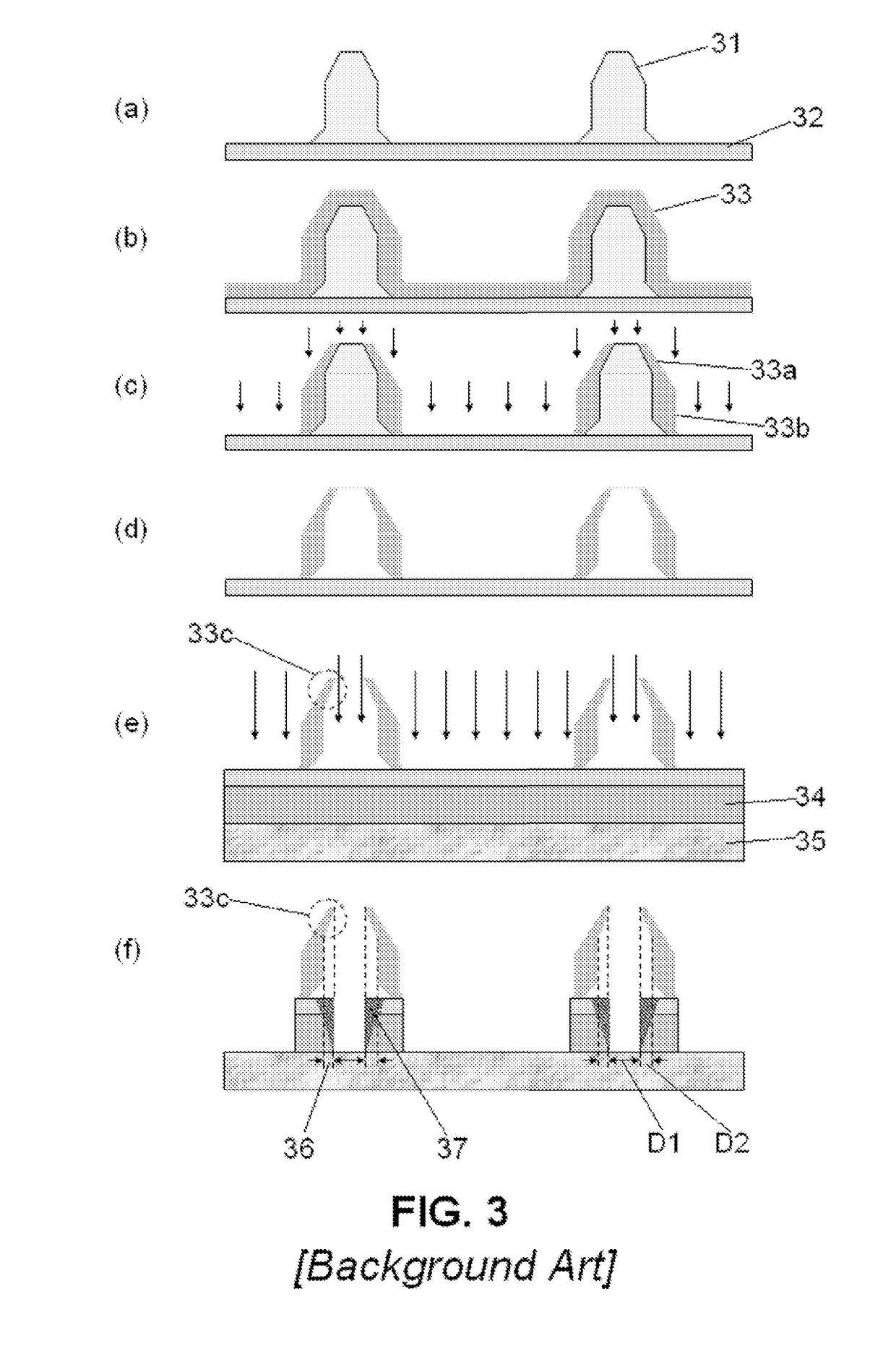
However, forming the pre-patterned feature having a flat top is extremely difficult and in reality, all pre-pattered features have at least a partially rounded top.
As a result, unavoidably the overhang portion of the spacer is formed, and due to the overhang portion, the distance 69 between the top edges of the spacer becomes smaller than that between inner vertical portions of the spacer.
However, that requires more processing steps and processing complexity, thereby increasing production cost.

Method used


Image

  • Method of depositing film with tailored comformality
  • Method of depositing film with tailored comformality
  • Method of depositing film with tailored comformality

Examples


examples

[0089]A flowable film was deposited using bis-diethylaminosilane (BDEAS) and no oxygen gas, and a conformal film was also deposited using bis-diethylaminosilane (BDEAS) and oxygen gas, in the same reactor under the conditions shown in Table 1.

[0090]

TABLE 1Flowable filmConformal filmdepositiondepositionProcessPulsed PECVDPEALDSusceptor temperature (° C.)2020Source vessel temperature (° C.)2525BDEAS flow rate (sccm)104Carrier Ar flow rate (sccm)400400Deposition pressure (Pa)300200Oxygen gas flow rate (sccm)0200Plasma power (W)40200

[0091]If separate reactors are used, the deposition conditions will be adjusted as shown in Table 2.

[0092]

TABLE 2Flowable filmConformal filmdepositiondepositionProcessPulsed PECVDPEALDSusceptor temperature (° C.)−2070Source vessel temperature (° C.)2525BDEAS flow rate (sccm)104Carrier Ar flow rate (sccm)400400Deposition pressure (Pa)300200Oxygen gas flow rate (sccm)10200Plasma power (W)4040

[0093]First, a substrate having a pre-patterned photoresist (made of ...


PUM

PropertyMeasurementUnit
temperatureaaaaaaaaaa
aspect ratioaaaaaaaaaa
widthaaaaaaaaaa

Abstract

A method of depositing a film with a target conformality on a patterned substrate, includes: depositing a first film on a convex pattern and a bottom surface; and depositing a second film on the first film, thereby forming an integrated film having a target conformality, wherein one of the first and second films is a conformal film which is non-flowable when being deposited and has a conformality of about 80% to about 100%, and the other of the first and second films is a flowable film which is flowable when being deposited.

Description

BACKGROUND[0001]1. Field of the Invention[0002]The present invention generally relates to a technology of depositing a film having a film thickness different at the top and bottom of a patterned surface of a substrate.[0003]2. Description of the Related Art[0004]Spacer defined double patterning (SDDP) technique has been developed for photolithography to enhance the feature density. The resolution of a photoresist pattern begins to blur at around 45 nm half-pitch. Thus, for the semiconductor industry, double patterning appears to be the only lithography technique to be used for nodes smaller than the 45 nm half-pitch nodes.[0005]Conventionally, SDDP was performed as illustrated in FIG. 3. First, pre-patterned features 31 (e.g., photoresist) are formed on a hard mask 32 as shown in FIG. 3(a). Next, a conformal spacer film 33 is deposited to cover the pre-patterned features 31 and the hard mask 32 as shown in FIG. 3(b). A spacer will be a film layer formed on a sidewall of the pre-patt...

Claims


Application Information

Patent Timeline
Patent Type & Authority Patents(United States)
IPC IPC(8): B44C1/22
CPCC23C16/325C23C16/345C23C16/401C23C16/45525C23C16/515H01L21/02164H01L21/02167H01L21/0217H01L21/02219H01L21/02274H01L21/0228H01L21/0234H01L21/02348H01L21/0337
Inventor HA, JEONGSEOK
Owner ASM JAPAN
Learn More