Methods for forming conformal oxide layers on semiconductor devices

a technology of conformal oxide and semiconductor devices, applied in semiconductor devices, electrical equipment, electric discharge tubes, etc., can solve the problems of poor device performance or failure, high wafer or substrate temperature required in thermal oxidation process, and silicon wafer dopants, etc., to increase the sticking coefficient of oxygen species

Active Publication Date: 2013-05-07
APPLIED MATERIALS INC
View PDF17 Cites 2 Cited by
  • Summary
  • Abstract
  • Description
  • Claims
  • Application Information

AI Technical Summary

Benefits of technology

[0009]One aspect of the present invention relates to a method of treating an oxide layer formed on a semiconductor substrate. According to one or more embodiments, the method includes placing such a substrate in a plasma reaction chamber on a substrate support. The chamber utilized in one or more embodiments includes an ion generation region. The method may also include introducing or flowing a process gas into the chamber where, in the ion generation region, a plasma is generated in the ion generation region of the chamber and is used to form an oxide layer on the substrate. The plasma formed according to one or embodiments may include oxygen or an oxygen species. In one or more embodiments, the oxide layer is formed from the plasma while the substrate is actively cooled. In such embodiments, actively cooling the substrate increases the sticking coefficient of the oxygen species included in some plasmas.

Problems solved by technology

Unfortunately, as feature sizes are becoming much smaller and different oxides are employed in the next generation of advanced technologies, the high wafer or substrate temperatures required in thermal oxidation processes are problematic in that the dopants in the silicon wafer (well doped and junctions) diffuse at the higher temperatures (e.g., above about 700° C.).
Such a distortion of the dopant profiles and other features can lead to poor device performance or failure.
Plasma processes used to form oxide layers have similar problems.
For example, at high chamber pressure (e.g., 100 mTorr), contaminants tend to accumulate in the gate oxide layer during formation, leading to fatal defects in the gate oxide structure such as dangling bonds or mobile charge, and at low chamber pressure (e.g., tens of mTorr), increased plasma ion energy leads to ion bombardment damage and other diffusion problems.
For example, conventional oxidation processes often result in a defect known as a bird's beak.
The intrusion of the oxide layer into the active region of the memory cell (e.g., in flash memory applications) reduces the active width of the memory cell, thereby undesirably reducing the effective width of the cell and degrading the performance of the flash memory device.
Another limitation of current low temperature plasma processes is that oxidation appears to occur preferentially on surfaces parallel to the wafer or substrate plane, namely, the top and bottom of structures such as gates formed by stacked layers of materials and trenches formed between the gates.
Regardless of the cause, limited oxidation occurs on the sidewalls of the stacks, resulting in an unacceptably thin sidewall layer on the gate stacks and poor conformality.

Method used


Image

  • Methods for forming conformal oxide layers on semiconductor devices
  • Methods for forming conformal oxide layers on semiconductor devices
  • Methods for forming conformal oxide layers on semiconductor devices

Examples


Embodiment Construction

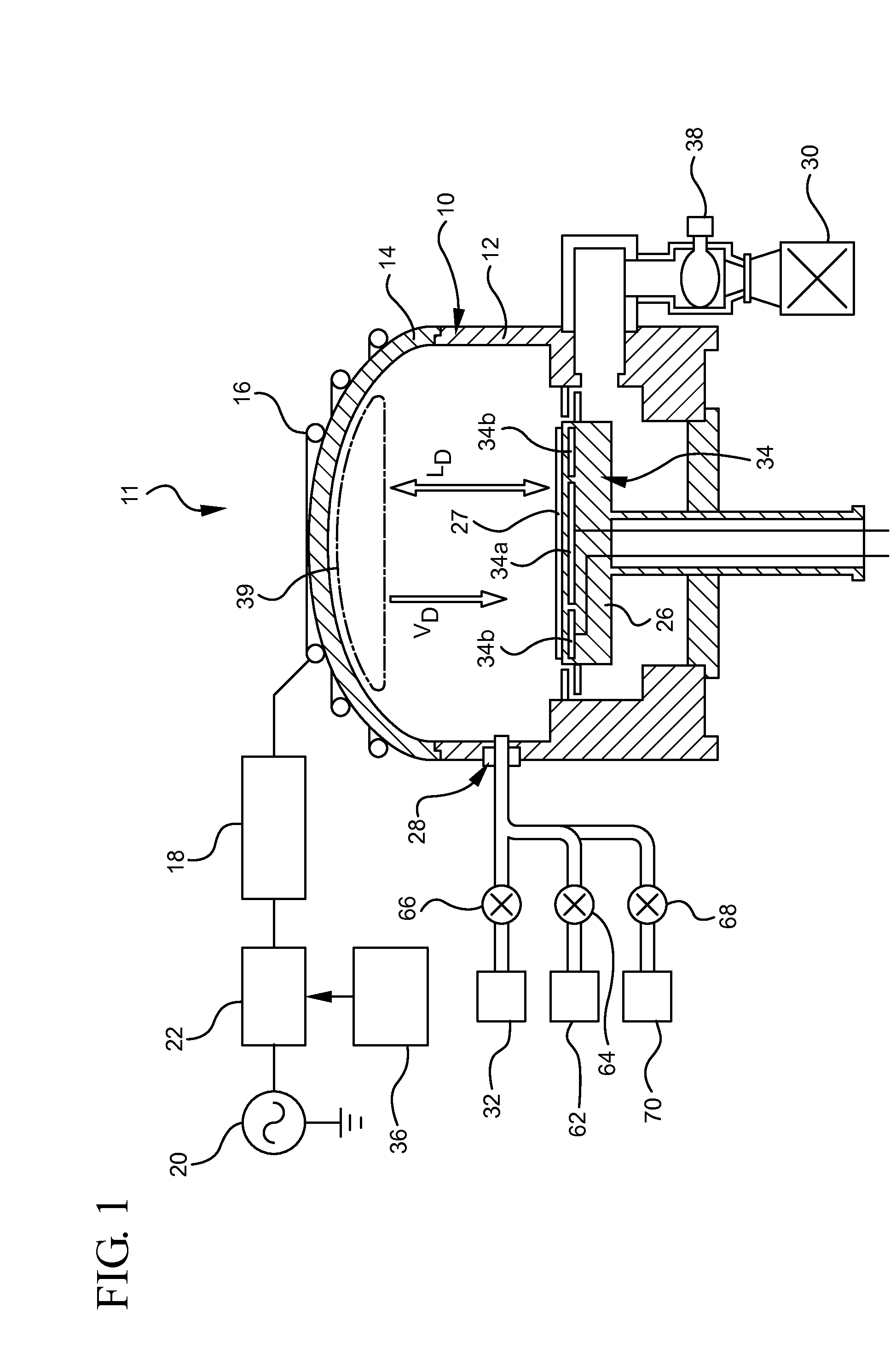
[0022]Embodiments of the present invention provide methods for forming conformal oxide layers by oxidation of semiconductor substrates. Specific embodiments described below are described with reference to oxide layers formed by low temperature oxidation.

[0023]As used herein, low temperature oxidation refers to oxidation at temperatures below about 700° C. Conventional plasma oxidation occurs at temperatures above 100° C. due to plasma power transferred to the substrate. At temperatures above 100° C., oxygen ion flux dominates the oxidation process and thus, only half of the oxidation flux arrives at vertical sidewalls, compared the oxidation flux that arrives on horizontal walls (which may also be referred to as top and bottom surfaces or gates and trenches) of structures having a width of 50 nm. Accordingly, where conformality is defined as the ratio of the growth on a sidewall and the growth on a top or bottom surface, conventional plasma oxidation achieves only a 50% conformality...


PUM


Abstract

Methods and apparatus for forming an oxide layer on a semiconductor substrate are disclosed. In one or more embodiments, plasma oxidation is used to form a conformal oxide layer by controlling the temperature of the semiconductor substrate at below about 100° C. Methods for controlling the temperature of the semiconductor substrate according to one or more embodiments include utilizing an electrostatic chuck and a coolant and gas convection.

Description

CROSS-REFERENCE TO RELATED APPLICATION[0001]This application claims priority to U.S. Provisional Application No. 61 / 147,908, filed Jan. 28, 2009, which is hereby incorporated by reference in its entirety.BACKGROUND OF THE INVENTION[0002]1. Field of the Invention[0003]Embodiments of the present invention generally relate to semiconductor fabrication, and more particularly, to oxidation of a semiconductor device or its components to form conformal oxide layers.[0004]2. Description of the Related Art[0005]Semiconductor devices require thin oxide layers to be formed at various stages of their fabrication. For example, in transistors, a thin gate oxide layer may be formed as part of a gate stack structure, including sidewalls, as will be described further below. In addition, in some applications, such as in the fabrication of a flash memory film stack, a thin oxide layer may be formed surrounding the entire gate stack, for example, via exposing the stack to an oxidation process. Such oxi...

Claims


Application Information

Patent Timeline
Patent Type & Authority Patents(United States)
IPC IPC(8): H01L21/31
CPCH01J37/321H01J37/32137H01J37/32724H01L21/0223H01L21/02238H01L21/02252H01L29/7881H01L21/28282H01L21/3165H01L21/31662H01L21/67109H01L21/76224H01L21/28273H01L29/40114H01L29/40117
Inventor TJANDRA, AGUS S.OLSEN, CHRISTOPHER S.SWENBERG, JOHANES F.YOKOTA, YOSHITAKA
Owner APPLIED MATERIALS INC
Why Eureka
Try Eureka