
Lateral trench transistor, as well as a method for its production

a technology of trench transistors and transistors, which is applied in the direction of basic electric elements, electrical equipment, semiconductor devices, etc., can solve the problems of high voltage drop across the area of the source region that is furthest away from the source, and the destruction of the trench transistor

Active Publication Date: 2013-04-30
INFINEON TECH AG
View PDF13 Cites 1 Cited by
  • Summary
  • Abstract
  • Description
  • Claims
  • Application Information

AI Technical Summary

Benefits of technology

[0011]The heavily doped semiconductor region allows charge which has been produced during the breakdown mode to flow away to the source contact via a low-impedance path. It is thus possible to reduce the resistance which the charges have to overcome. This likewise reduces the voltage drop produced by the charge carriers, so that it is possible to prevent a parasitic transistor comprising the source region, the body region and the drain region from being switched on.
[0014]If the source contact is located on the upper face of the semiconductor body, then the heavily doped semiconductor region is expediently made contact with only on the upper face of the semiconductor body. However, if the source contact extends into the semiconductor body, then the heavily doped semiconductor region can expediently be designed in such a way that it is adjacent to the source contact over the entire penetration depth of the heavily doped semiconductor region. This makes it possible to further reduce the resistance which the charge carriers have to overcome before reaching the source contact.
[0025]The dopants can be driven out by one or more heat-treatment processes after introduction into the semiconductor body. This means, for example, that it is possible to define the different extent of the source region and body region with respect to one another, and thus to set the channel length of the body region to a desired value.

Problems solved by technology

The holes which are generated when a lateral trench transistor such as this is in the breakdown state, have to pass through the body region, which runs alongside the source region and extends over the entire trench depth, to the source contact and, if the trench depth is sufficient, the generally high layer resistance of the body region results in a high voltage drop across the area of the source region which is furthest away from the source contact.
This can in turn lead to destruction of the trench transistor.

Method used


Image

  • Lateral trench transistor, as well as a method for its production
  • Lateral trench transistor, as well as a method for its production
  • Lateral trench transistor, as well as a method for its production

Examples


first embodiment

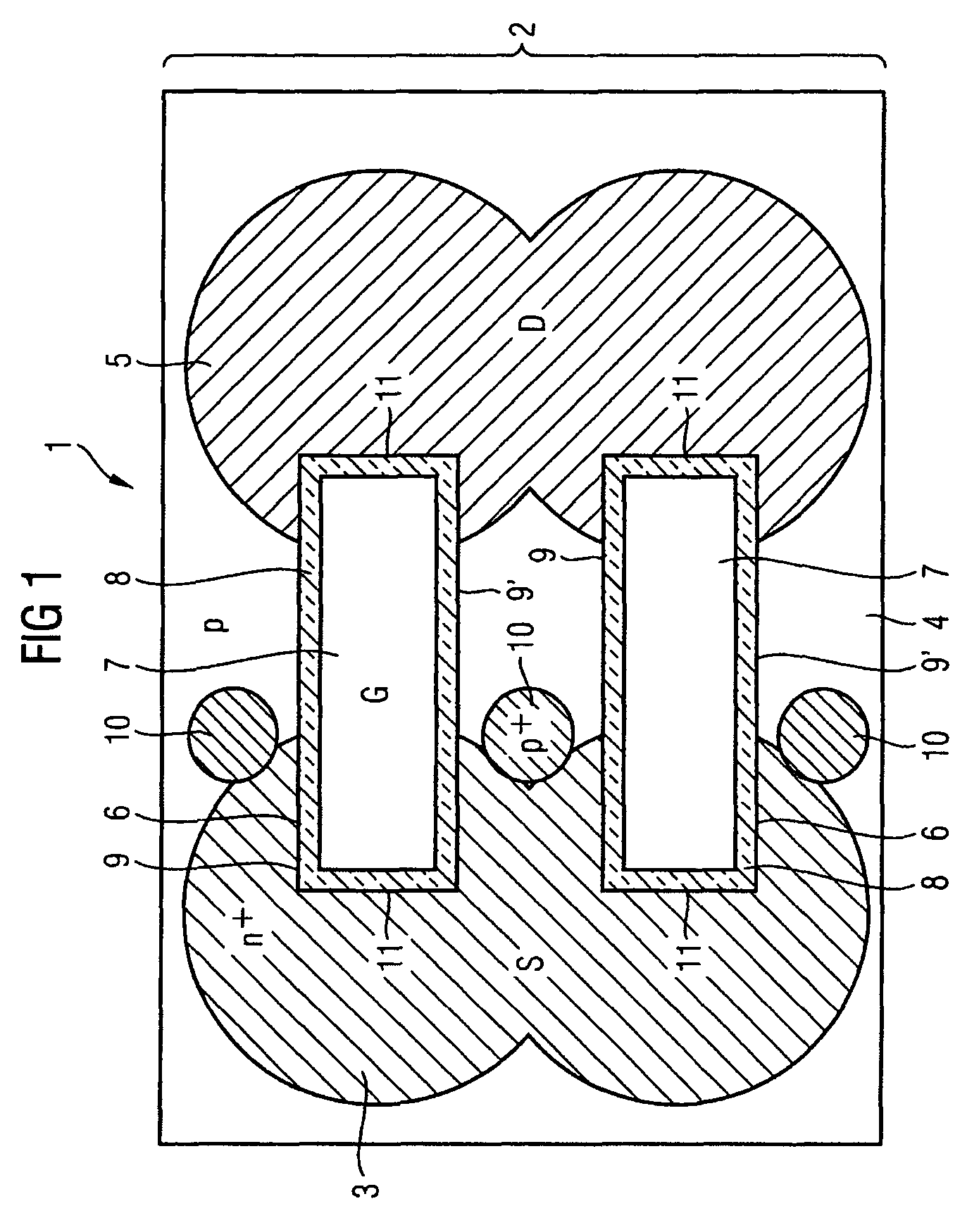
[0044]FIG. 1 shows the lateral trench transistor according to the invention. A lateral trench transistor 1 has a semiconductor body 2 in which an n30 -doped source region 3 and a p-doped body region 4, with which contact is made by means of a source contact (which is not shown here), an n30 -doped drain region 5 and a gate trench 6, in which a gate electrode 7 is embedded, are provided. The gate electrode 7 is electrically isolated from the semiconductor body 2 by an isolation layer 8.

[0045]In this embodiment, a plurality of gate trenches 6 are provided and are arranged parallel to one another, with in each case one end of a gate trench 6 ending in the source region 3, and one end of the gate trench 6 ending in the drain region 5. The gate electrodes 7 allow current flows along the gate trench side walls 9 between the source region 3 and the drain region 5 to be controlled / produced.

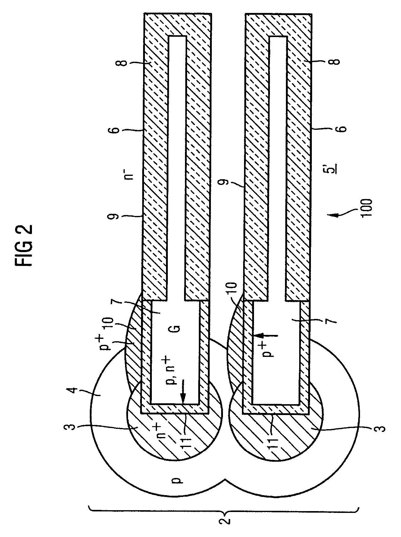
[0046]Furthermore, p30 -doped semiconductor regions 10 are formed within the body region 4 and penetra...

third embodiment

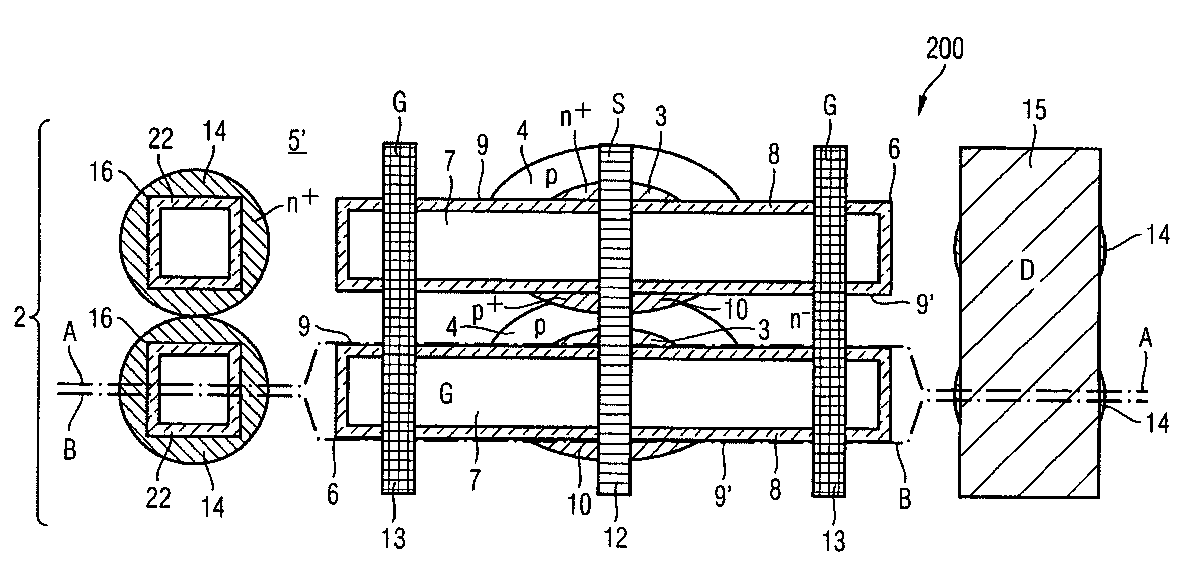
[0048]FIG. 3 shows the lateral trench transistor according to the invention. A lateral trench transistor 200 has a plurality of gate trenches 6, in each of which one gate electrode 7 is embedded. The gate electrodes 7 are electrically isolated from the semiconductor body 2 via appropriate isolation layers 8. Furthermore, source regions 3 are provided, with each source region being adjacent to one gate trench side wall 9. Each source region 3 is embedded in one body region 4, with each body region being adjacent to the same gate trench side wall 9 to which the corresponding source region 3 is also adjacent. Heavily doped semiconductor regions 10 whose dopant type corresponds to the dopant type of the body regions 4 are in each case adjacent to a gate trench side wall 9′, which is opposite the gate trench side wall 9 to which the body regions and source regions are adjacent. Each body region 4 overlaps a heavily doped semiconductor region 10. This ensures that holes which are produced...


PUM


Abstract

A lateral trench transistor has a semiconductor body having a source region, a source contact, a body region, a drain region, and a gate trench, in which a gate electrode which is isolated from the semiconductor body is embedded. A heavily doped semiconductor region is provided within the body region or adjacent to it, and is electrically connected to the source contact, and whose dopant type corresponds to that of the body region.

Description

FIELD OF THE INVENTION[0001]The invention relates to a lateral trench transistor and to a method for production of semiconductor regions in a semiconductor body of a lateral trench transistor.BACKGROUND OF THE INVENTION[0002]Lateral trench transistors are known; in one specific embodiment, they have a semiconductor body in which a source region and a body region, with which contact is made by means of a source contact, a drain region, with which contact is made by a drain contact, and a gate trench, in which a gate electrode which is isolated from the semiconductor body is embedded, are provided. Lateral current flows between the source region and the drain region along a side wall of the gate trench can be produced and controlled by means of the gate electrode.[0003]The holes which are generated when a lateral trench transistor such as this is in the breakdown state, have to pass through the body region, which runs alongside the source region and extends over the entire trench dept...

Claims


Application Information

Patent Timeline
Patent Type & Authority Patents(United States)
IPC IPC(8): H01L29/66
CPCH01L29/1045H01L29/1095H01L29/66689H01L29/66704H01L29/78H01L29/7825H01L29/66666H01L29/4236H01L21/26586H01L29/0696H01L29/41758H01L29/42368
Inventor HIRLER, FRANZWAHL, UWEMEYER, THORSTENRUB, MICHAELWILLMEROTH, ARMINSCHMITT, MARKUSTOLKSDORF, CAROLINSCHAFFER, CARSTEN
Owner INFINEON TECH AG
Learn More