


Quick Research
Generate reliable direction feasibility study reports for your R&D in just a few steps.

Technical Q&A
Discover and master advanced knowledge NOW. Basics, ideas, possibilities, all at once.

Find Solutions
As an expert in R&D theories, this can generate solutions to your technical problems instantly.

Evaluate Feasibility
Analyze your overall solution with one click, know your potential R&D risks in advance.

Monitor Landscape
Get weekly tech updates, stay abreast of the latest tech innovations and key insights.
Method and apparatus for data processing in mobile communication system
a mobile communication system and data processing technology, applied in the field of mobile communication systems, can solve the problems of large data size, large cache memory size, and slow memory access speed, and achieve the effect of high-speed data processing
- Summary
- Abstract
- Description
- Claims
- Application Information
AI Technical Summary
Benefits of technology
Problems solved by technology
Method used
Image


Examples
first embodiment
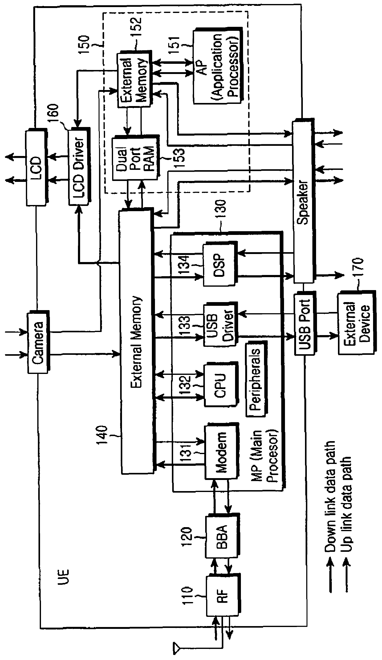
[0039]FIG. 5 illustrates a structure of a UE according to the present invention, which corresponds to a structure supporting basic parallel processing.
[0040]Referring to FIG. 5, the UE includes memories divided into an external memory 510 and an internal memory 580, and a multi-layer bus matrix 570 designed to enable the external memory 510 and the internal memory 580 to independently operate. Although FIG. 5 shows a CPU 530, a modem 540, an external interface device 550, and an encryption / decryption block 560 as examples of IP blocks, other IP blocks can also be connected in the same way. Further, the UE illustrated in FIG. 5 uses a single internal memory 580, and each of the IP blocks 540, 550, and 560 can access the internal memory 580 through the bus matrix 570. Also, although the internal memory 580 of the UE illustrated in FIG. 5 has one port, the UE may use a Dual Port Random Access Memory (DPRAM) having two ports, which enables two IP blocks to simultaneously access the inte...
second embodiment
[0043]FIG. 6 illustrates a structure of a UE according to the present invention, which corresponds to a structure capable of simultaneously performing a downlink process and an uplink process.
[0044]Referring to FIG. 6, the UE according to the second embodiment of the present invention includes two internal memories divided into a downlink memory 610 and an uplink memory 620. Each of the memories 610 and 620 is connected to the bus matrix 630, so that two IP blocks can simultaneously access the internal memory 610 or 620. Further, as in the embodiment shown in FIG. 5, four IP modules can access the internal memory while performing the data process if a DPRAM is used as the internal memory.
third embodiment
[0045]FIG. 7 illustrates a structure of a UE according to the present invention, which corresponds to a structure capable of simultaneously performing sub-processes of a downlink process and an uplink process.
[0046]Referring to FIG. 7, the UE according to the third embodiment of the present invention includes two dual port memories used as internal memories, which are divided into a downlink memory 710 and an uplink memory 720. Each of the memories has one port connected to the bus matrix 730 and another port connected through a direct bus to an IP block, such as a modem 760, an external interface device 750, and an encryption / decryption block 740. By this structure, not only can four IP blocks simultaneously access the internal memory to perform data processes, but also, two ports can directly access IP blocks without passing the bus matrix 730, and thus can perform an independent process. Although the encryption / decryption block 740 and the external interface device 750 are connec...
PUM
 Abstract
Description
Claims
Application Information
 - R&D Engineer
- R&D Manager
- IP Professional
- Industry Leading Data Capabilities
- Powerful AI technology
- Patent DNA Extraction
Browse by: Latest US Patents, China's latest patents, Technical Efficacy Thesaurus, Application Domain, Technology Topic, Popular Technical Reports.
© 2024 PatSnap. All rights reserved.Legal|Privacy policy|Modern Slavery Act Transparency Statement|Sitemap|About US| Contact US: help@patsnap.com