
Integrated circuit package component and ball grid array simulation model

a simulation model and integrated circuit technology, applied in the field of simulation models of electronic components, can solve the problems of increasing complexity, limited software tools, and current modeling of flip-chip bgas using expensive and complex software tools, and achieve the effect of effective ic package component design

Inactive Publication Date: 2013-02-26
XILINX INC
View PDF3 Cites 6 Cited by
  • Summary
  • Abstract
  • Description
  • Claims
  • Application Information

AI Technical Summary

Benefits of technology

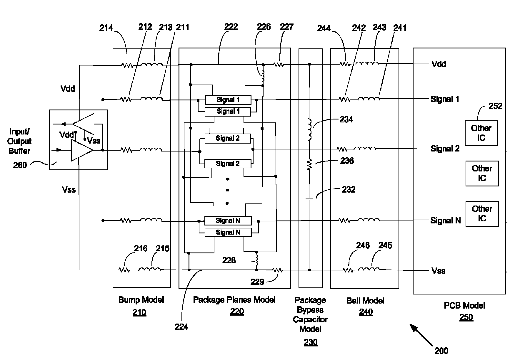
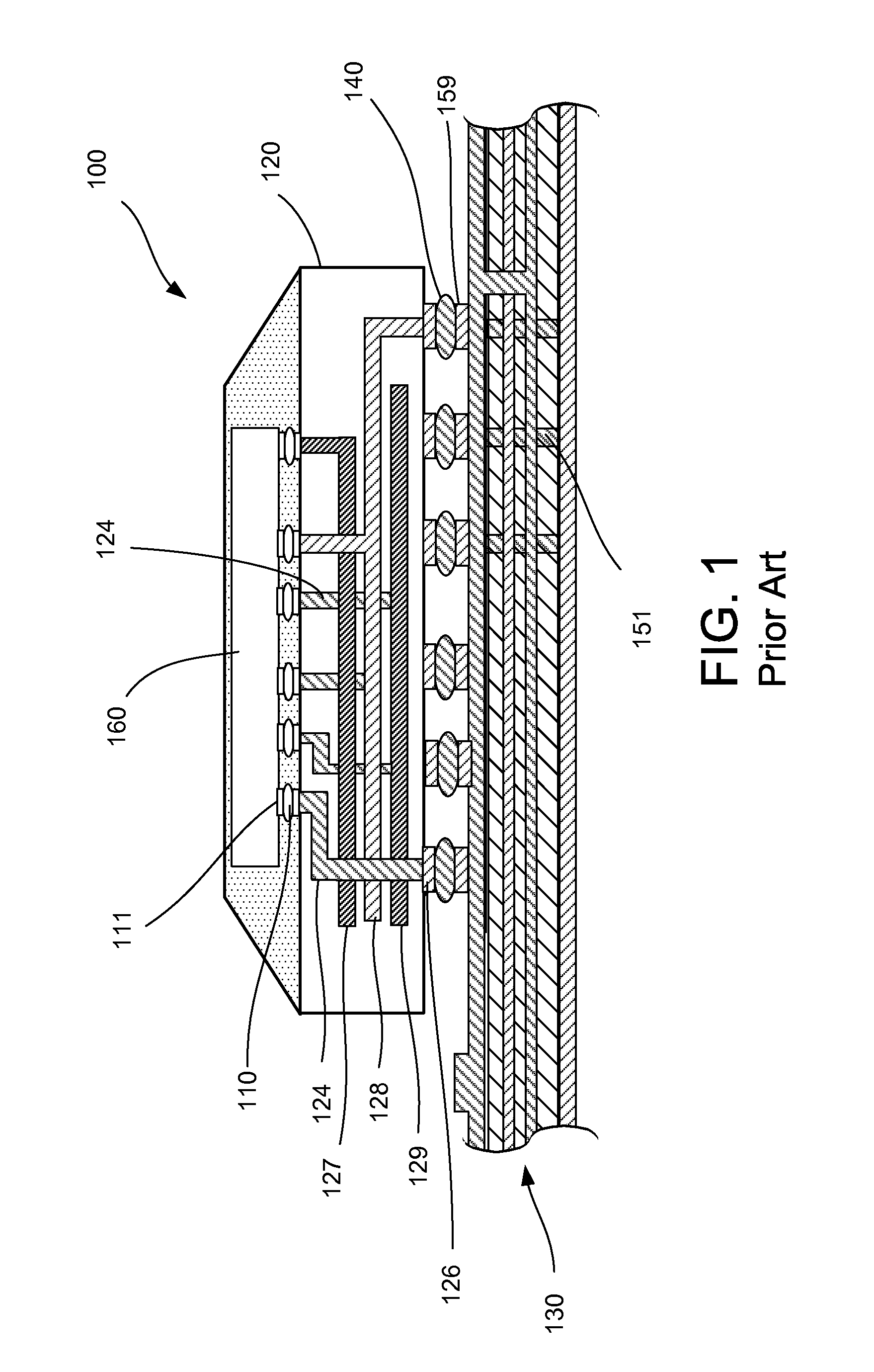
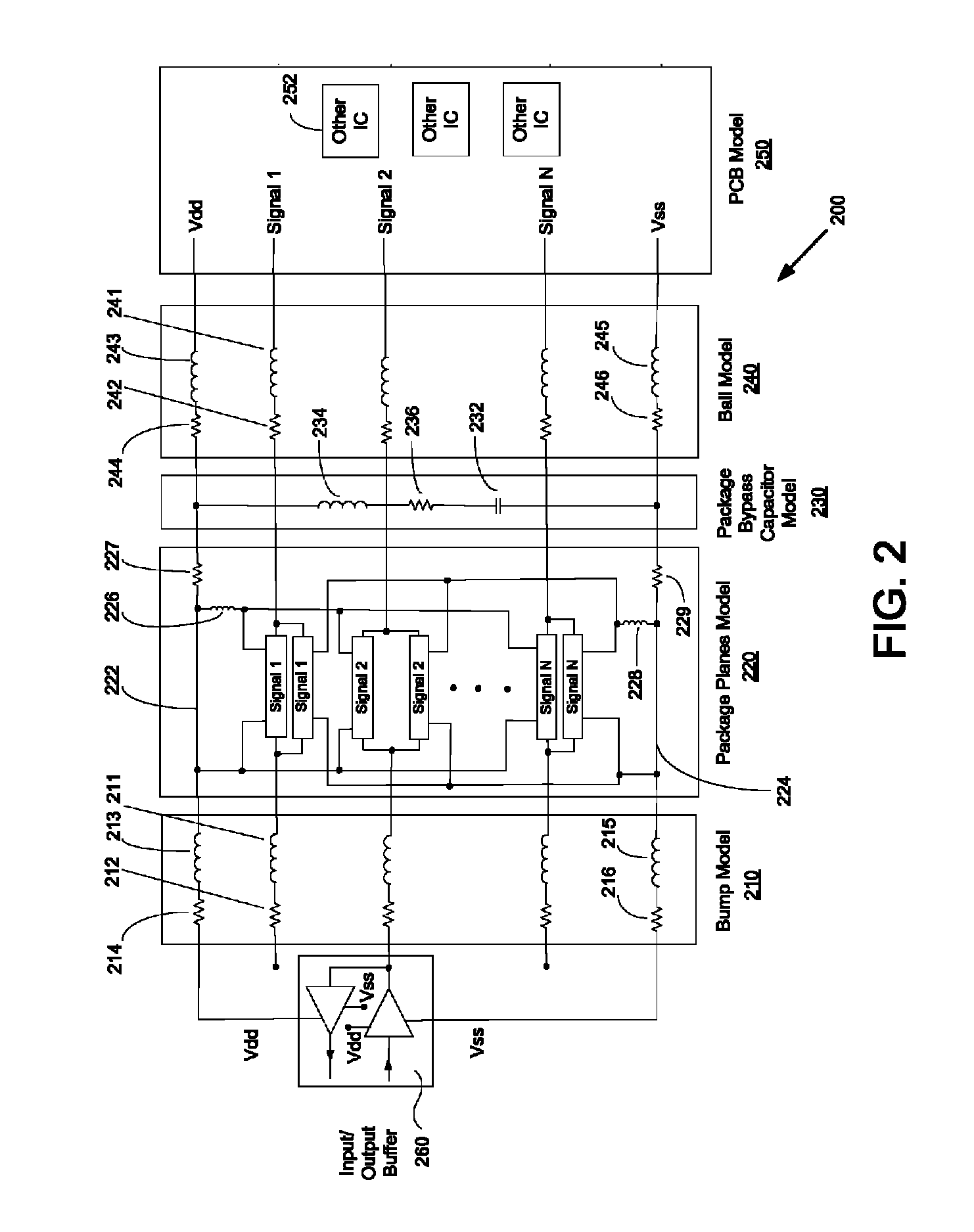
The present invention provides a simulation model for flip-chip BGAs that helps engineers understand the impact of power supply droop, ground bounce, and crosstalk between adjacent signals on the package and system levels. The model includes resistors, inductors, capacitors, and transmission lines to simulate the electrical interaction between signal conductors, power / ground planes, vias, and balls in a flip-chip package. The model helps engineers design more effective IC packages and understand the actual physical effects of flip-chip and IC package interactions.

Problems solved by technology

As ICs have gotten faster with smaller and smaller feature sizes, they have also gotten much more complex.
Modern, highly complex, ICs can and often do include hundreds of Input / Output structures and associated connection infrastructure, such as bonding pads for example, that access the device's logical circuitry.
However, current modeling for flip-chip BGAs requires use of expensive and complex software tools.
These software tools are limited because they employ a finite element method analysis, and thus there are not enough elements available to adequately simulate current flip-chip BGAs.
Further, these software tools require a lot of computing power for simulations.
Still further, these software tools are time consuming, leaving engineers with very little time to analyze and address design concerns, and don't enable engineers to fully understand the impacts and effects of power supply droop, ground bounce and crosstalk between adjacent signals either at the package level or at the system level.

Method used


Image

  • Integrated circuit package component and ball grid array simulation model
  • Integrated circuit package component and ball grid array simulation model
  • Integrated circuit package component and ball grid array simulation model

Examples


Embodiment Construction

[0016]Reference will now be made in detail to embodiments of the present invention, examples of which are illustrated in the accompanying drawings. While the invention will be described in conjunction with these embodiments, it will be understood that they are not intended to limit the invention to these embodiments. On the contrary, the invention is intended to cover alternatives, modifications and equivalents, which may be included within the spirit and scope of the invention as defined by the appended claims. Furthermore, in the following detailed description, numerous specific details are set forth in order to provide a thorough understanding of the present invention. However, it should be understood by one of ordinary skill in the art that the present invention may be practiced without these specific details. In other instances, well-known methods, procedures, components, and circuits have not been described in detail so as not to unnecessarily obscure aspects of the present in...


PUM


Abstract

A simulation model is provided for flip-chip BGAs to help engineers determine the effects of IC package components. The simulation model includes a bump model, a package planes model, a package bypass capacitor model, a ball model and a PCB model. The simulation model in particular includes resistors, inductors, capacitors and transmission lines to simulate the electrical interaction between signal conductors, power / ground planes, vias and balls that exist in a flip-chip ball grid array (BGA) package. The simulation model helps engineers understand actual physical effects of flip-chip and IC package interactions, as well as the impact of the effects of power supply droop, ground bounce and crosstalk between adjacent signals, not only on the IC package level, but at the computer system level.

Description

FIELD OF THE INVENTION[0001]Embodiments of the present invention relate to simulation models for electronic components such as integrated circuits, particularly integrated circuit packages with external connections to the package formed by a ball grid array.BACKGROUND OF THE INVENTION[0002]An integrated circuit (IC) device typically includes an IC chip that is housed in a plastic, ceramic or metal package. The IC chip typically includes a circuit fabricated by lithographically patterning conductive and insulating materials on a thin wafer of semiconductor using known fabrication techniques. The package supports and protects the IC chip and provides electrical connections between the circuit and an external circuit or system.[0003]It is important to note that a design of an integrated circuit device cannot be verified by “bread-boarding” but must be simulated. Simulation of Integrated circuits is commonly implemented with a SPICE program (Simulation Program with Integrated Circuit Em...

Claims


Application Information

Patent Timeline
IPC IPC(8): G06F17/50G06G7/62
CPCG06F17/5036G06F2217/40G06F2113/18G06F30/367
Inventor ANDERSON, RAYMOND E.MEHTA, SANJAY S.WHEELER, RICHARD L.
Owner XILINX INC
Learn More