
Low inductance contact probe with conductively coupled plungers

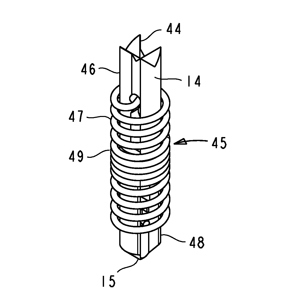
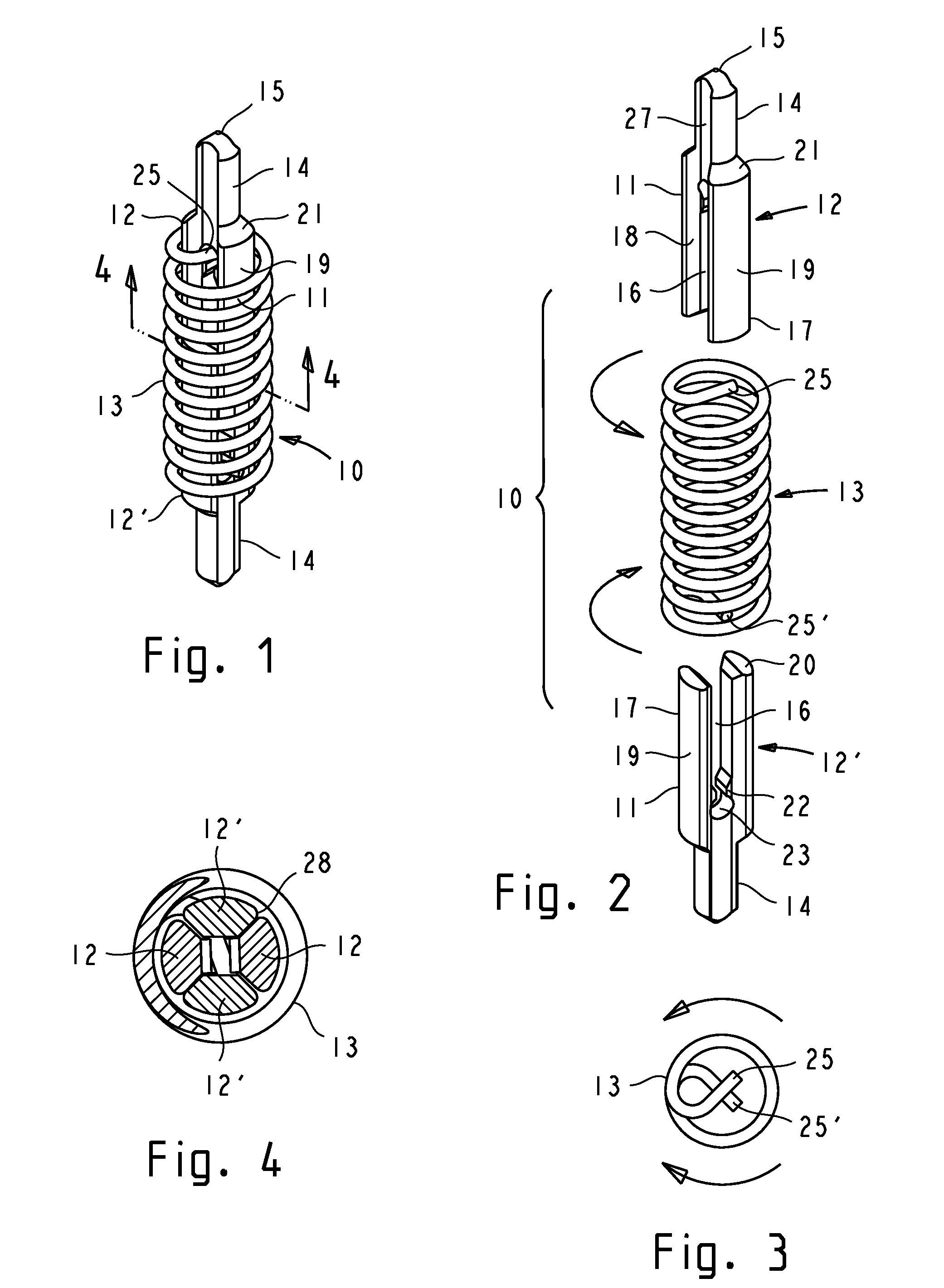
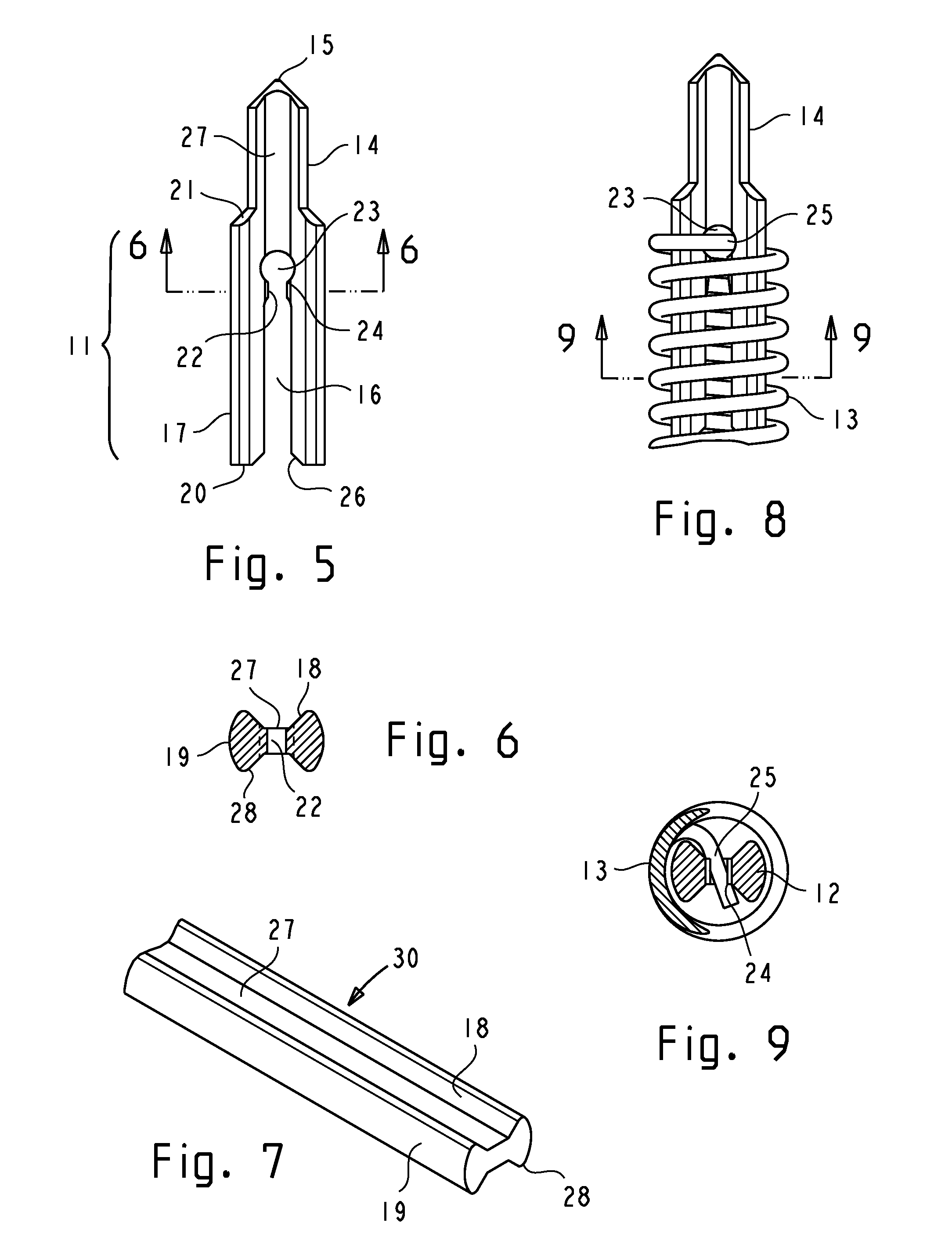
a plunger and contact probe technology, applied in the field of low inductance contact probes, can solve the problems of premature contact probe failure, accelerated wear of contacting surfaces, and reduced overall contact resistance of the probe, and achieve the effect of substantially reducing the parasitic electrical effect of the spring

Inactive Publication Date: 2013-02-12
SOCHOR JERZY ROMAN
View PDF13 Cites 65 Cited by
  • Summary
  • Abstract
  • Description
  • Claims
  • Application Information

AI Technical Summary

Benefits of technology

The patent describes a design for a conductive contact that reduces the effects of parasitic electromagnetic effects caused by the spring used in the device. The plungers are connected together using a spring that prevents rotation, which results in a torsional bias that pushes the plungers together and creates a direct conductive path. This design can be fabricated using a drawn profiled wire and is highly tolerant to misalignment. Overall, this design improves the accuracy and reliability of the conductive contact.

Problems solved by technology

This creates a conductive shunt which significantly lowers the overall contact resistance of the probe and the parasitic electrical effects of the coil spring.
Since the contact between the plunger and the bore of the barrel is localized along the line of contact where the edge of the plunger traverses the bore of the barrel, an excessive tilt often causes accelerated wear of contacting surfaces and a premature contact probe failure.
However, miniaturization of contact probes often leads to compliance problems since the small probes tend to have a low deflection capability, while the manufacturing tolerances, assembly tolerances, and board planarity, do not scale accordingly and remain substantially the same as for larger contacts.
However, a coil spring acts as an electrical inductor at high frequencies and therefore presents electrical performance problems.
On the other hand, the pointing accuracy becomes more difficult to control in small contact probes as the plunger-to-barrel diametrical clearance is likely to have more impact on tilting of the plunger, especially when the plunger bodies which are guided in the barrel become very short.
While the random tilting of the plungers enables the plunger-to-barrel contact, it adversely affects the probe's pointing accuracy.
While the spring characteristics is usually linear, the friction can lead to non-linear or erratic forces.
In the case of the tilted plungers in sliding contact with the bore, the bore surface is often irregular and the contact force between the edge of the plunger and the bore of the barrel is difficult to control.
In severe cases, gauging of surfaces may expose bare metal, cause oxidation of surfaces and accumulation of a nonconductive debris between contact surfaces.
This will cause high contact interface resistance and / or high friction forces which can cause a plunger to seize in the bore.
Plating of high aspect ratio and small diameter barrels creates challenges due to the difficulty of circulating the plating solution through a small bore.
Furthermore, the in-process quality control of the plating inside the barrel is difficult as the plating uniformity and thickness can only be evaluated by cutting the barrel lengthwise to expose the bore.
In addition, the base surface of the bore is often irregular and difficult to clean thoroughly prior to plating.
If the probe length is short, the probe design, materials, and contact forces have significant impact on the cycle life of the probe and tradeoffs are necessary.
However, music wire is made from a high carbon steel, is magnetic, and has low electrical conductivity.
While very reliable and durable probes can be produced in larger sizes, the desired probe characteristics is difficult to achieve in miniature probes, e.g., probes having an outside diameter of less than 1.0 mm and the length of less than 5 mm.
In view of the machining tolerances and plating thickness variation on the inside of the barrel and on the plunger, the diametrical fit between the plunger and the barrel is difficult to tightly control.
Since the plunger bodies which are guided in the bore of the barrel tend to be short, even a small diametrical clearance between the plunger and the bore can cause an excessive tilt of the plunger.
The excessive plunger tilt can lead to a high localized wear and increased friction which may cause seizing of the plunger in the barrel, preventing return of the plunger to the original extension, and thus causing a premature contact failure.
The surface defects and plating irregularities can significantly affect the sliding friction.
This can lead to large variation in contact forces and cause damage to the I / O terminals (e.g. deformation or shearing of BGA solder balls) when the contact forces are excessive.
The bottom of the barrel must be reliably plated, which is difficult, especially when small diameter, large aspect ratio barrels are used.
The deep drawn barrel can only provide an integral bull-nosed contact since pointed tips cannot be produced by the deep drawing process.
Such springs have a non-linear force vs deflection characteristics and can introduce a substantial variation in contact force and inductance due to manufacturing tolerances and non-planarity of mating interfaces.
In worst tolerance cases, at a maximum deflection condition the contact force can be excessive, while at a minimum deflection condition an insufficient number of coils may be shorted so that the inductance can be excessively high.
While such contact can provide an excellent electrical performance, it is not scalable to smaller sizes without a significant loss of compliance (deflection capability).
Furthermore, the contact is not easily adaptable for use with a variety of plungers which are often needed to adapt the contacts to a particular I / O terminal configuration, such as a solder ball of a BGA device.
(Although this quickly leads to excessively long contact probes with a high self-inductance.)
The recent increases in circuit integration and operating frequencies pushed the available probes and contacts to their performance limits.
While particular known contacts and probes have addressed some of the needs with various degree of success, none combine all the desired features in a single design.

Method used


Image

  • Low inductance contact probe with conductively coupled plungers
  • Low inductance contact probe with conductively coupled plungers
  • Low inductance contact probe with conductively coupled plungers

Examples


Embodiment Construction

[0077]The contact probes disclosed are of the type that are primarily used in an interposer type connector, wherein each contact is compressibly interposed between opposing terminals of a first device and a second device. “First device” and “first array” will generally refer to the device that is being plugged or connected whereas “second device” and “second array” will generally refer to the next level device or hardware to which the first device is being disengageably connected, usually represented by a PCB. The “first plunger” is disposed to contact the first device and is shown on the top side of the contact probe drawings, whereas the “second plunger” is disposed to contact the second device and is shown on the bottom side of the contact probe drawings. Otherwise, a contact probe can have identical, interchangeable plungers and the devices can have identical terminal pattern (e.g., LGA pads). In the cases where the plungers are identical or have substantially similar features, ...


PUM

PropertyMeasurementUnit
Angleaaaaaaaaaa
Forceaaaaaaaaaa
Angleaaaaaaaaaa

Abstract

A low inductance contact probe comprises conductively coupled plungers. The plungers have coupling means which enable them to be slidably and non-rotatably engaged. A coil spring is attached to the plungers in a manner that prevents rotation of the spring's ends. The spring provides an axial plunger bias, and a torsional bias for conductive coupling between the plungers. The torsional bias is generated by an axial displacement of the spring and by twisting the spring a predetermined angle prior to attachment to the plungers. Torsion-induced contact forces between the plungers assure a direct conductive path through the plungers. The torsional bias further enables a positive attachment of the spring to the plungers. Plungers with hermaphroditic coupling means can be fabricated from a drawn profiled stock by stamping or machining. Essential plunger coupling features can be prefabricated in a drawn profiled stock with a high degree of dimensional accuracy and reproducibility.

Description

BACKGROUND OF THE INVENTION[0001]1. Technical Field[0002]The present invention relates generally to electrical test probes and contacts for interconnecting integrated circuit (IC) devices and electronic components and systems, and specifically, to miniature high speed circuit probes and contacts having a low inductance and a low resistance. Applications include a test socket for connecting a ball grid array (BGA) IC package or a land grid array (LGA) IC package to a test system board; a socket for connecting an electronic device to a next level electronic hardware, battery and charging contacts, or other applications requiring low inductance and low contact resistance. The sockets can be used in an interposer configuration which provides separable interfaces for two oppositely disposed components having corresponding patterns (e.g., LGA to LGA or BGA to LGA) or, alternatively, the contacts can be permanently attached to a printed circuit board (PCB) or a system motherboard and provi...

Claims


Application Information

Patent Timeline
IPC IPC(8): G01R1/067H01R12/00H01R43/16
CPCH01R13/2421G01R1/06722H01R12/7082H01R12/714Y10T29/49204G01R1/06733H01R2201/20
Inventor SOCHOR, JERZY ROMAN
Owner SOCHOR JERZY ROMAN
Learn More