Manufacturing method of leadframe and semiconductor device

a manufacturing method and leadframe technology, applied in semiconductor devices, semiconductor/solid-state device details, electrical apparatus, etc., can solve the problems of reducing the reliability of semiconductor devices, generating >, and removing plating burrs reliably, so as to reduce the etching accuracy, prevent defects, and remove plating burrs.

Active Publication Date: 2013-01-08
ADVANCED SEMICON ENG INC
View PDF5 Cites 0 Cited by
  • Summary
  • Abstract
  • Description
  • Claims
  • Application Information

AI Technical Summary

Benefits of technology

[0015]According to the first aspect of the invention, a plating burr removal suitable to the etched area on which the half etching is performed and a plating burr removal suitable to the outer frame area on which pilot holes are provided so as to surround the unit lead frames in the leadframe material can be separately selected by selecting the plating burr removal based on the shape and material of the leadframe. As a result, it is possible to remove the plating burrs efficiently and reliably while preventing deformation of the leadframes.
[0044]Further, by selecting the platting burr removal based on the shape and material of the leadframe, it is possible to remove the plating burrs reliably and to prevent defects such as deformation of the lead frame. As a result, occurrence of defects can be prevented.

Problems solved by technology

However, in this manufacturing method, there is a problem that plating burrs 62,63 are generated due to erosion by etching solution at edges of the upper terminal portions 60 and the outer frame 53 that are protruded in the first etching step.
Further, they could affect etching accuracy in later stages, resulting in a problem of decrease in reliability of the semiconductor devices such as causing a short circuit.
Further, when the ultrasonic wave is used instead of the water jet, another problem could be caused that the leadframe is deformed because the strength is low in the half-etching area which is formed by reducing the thickness of the leadframe material by the etching conducted in the first etching step.
Thus, any of these means for removing the plating burrs are not sufficient to remove the plating burrs reliably over the entire surface of the leadframe.

Method used


Image

  • Manufacturing method of leadframe and semiconductor device
  • Manufacturing method of leadframe and semiconductor device
  • Manufacturing method of leadframe and semiconductor device

Examples


first embodiment

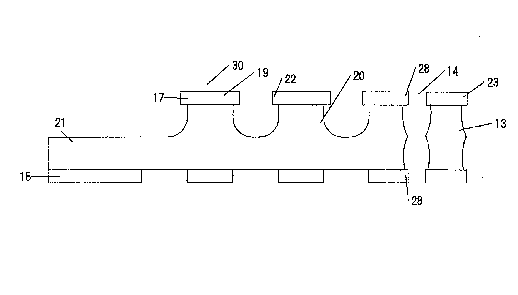
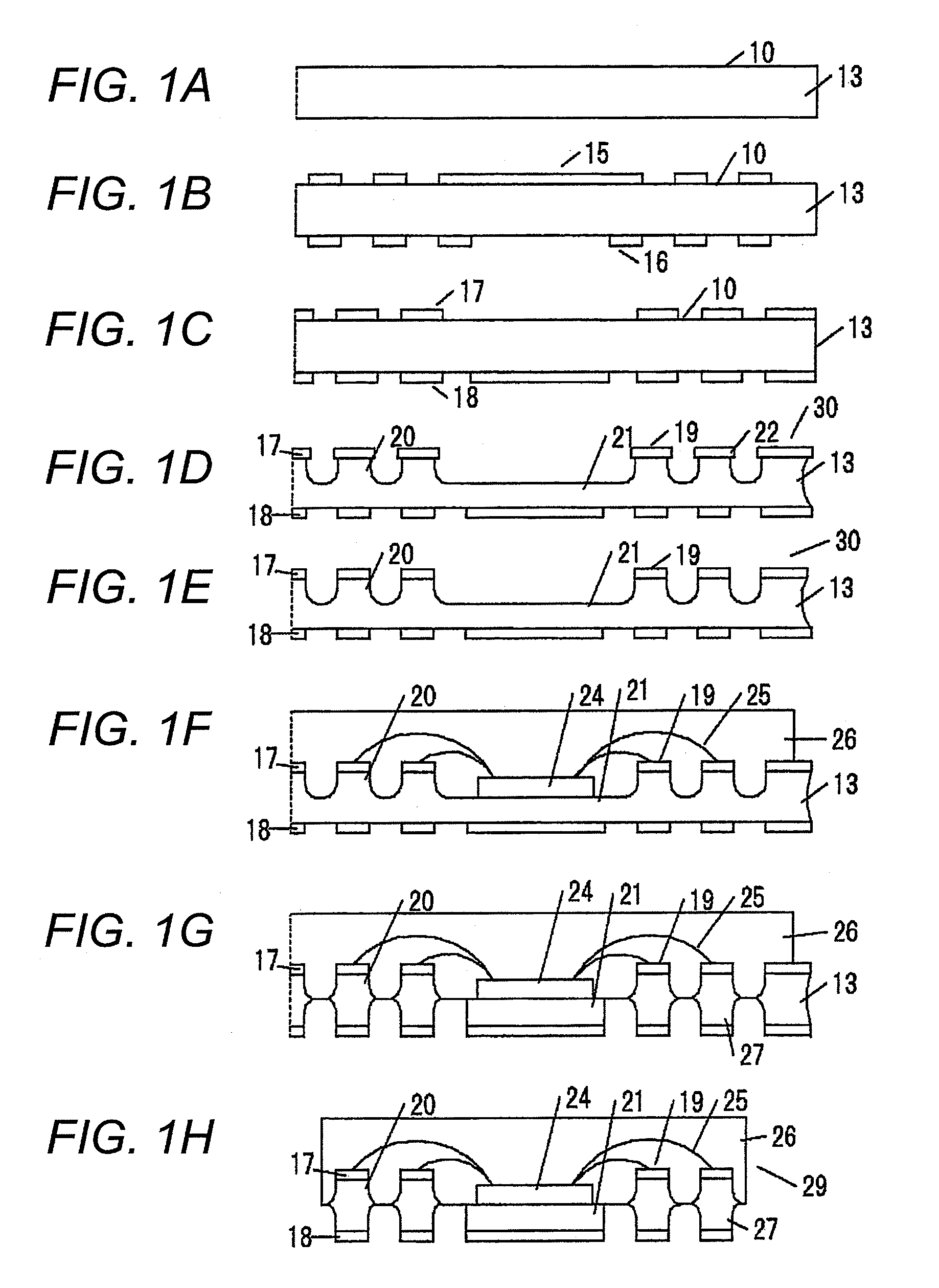
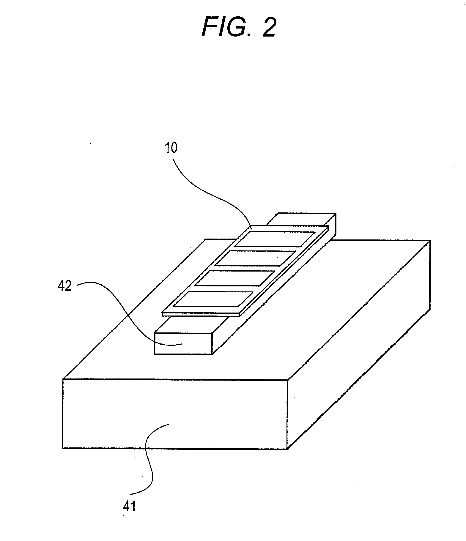
[0054]FIGS. 1A to 1H are explanatory views of steps in a manufacturing method of semiconductor devices according to a first embodiment of the invention. FIG. 2 is a perspective view showing a step of removing plating burrs by using ultrasonic waves according to the first embodiment. FIG. 3 is a plan view of a leadframe according to the first embodiment of the invention. FIG. 4 is a cross-sectional view of the leadframe before plating burr removal according to the first embodiment of the invention.

[0055]The step shown in FIG. 1A is a step of preparing a leadframe material. A leadframe material 10, which is referred to the area shown in the cross sectional view along the line X-X′ in FIG. 3, is constituted by a material of cupper or cupper alloy (or iron-nickel alloy, aluminum, aluminum alloy etc.) having a predetermined area. In this first embodiment, a single or a plurality of frame batches 12 having a plurality of unit leadframes 11 and an outer frame 13 around the frame batches 12...

second embodiment

[0070]The manufacturing method of semiconductor devices according to the second embodiment is the method in which the step of removing burrs in the first embodiment shown in FIG. 2 is modified with the step as described below. The other steps in the second embodiment are identical to those in the first embodiment. Therefore, description is omitted for these steps.

[0071]FIG. 6 is a perspective view showing a step of removing plating burrs by using ultrasonic waves according to the second embodiment.

[0072]Similarly to the first embodiment, the step of removing burrs in the second embodiment is conducted as shown in FIG. 1E. The plating burrs 23 on the outer frame 13 and the plating burrs 28 in the pilot holes 14 in the leadframe 30 shown in FIG. 3 are removed by applying ultrasonic waves to the areas where the plating burrs 23, 28 are formed to generate cavitation in the washing liquid. As shown in FIG. 6, the leadframe material 10 is disposed on a protection member 42 that is dispose...


PUM


Abstract

In order to remove plating burrs generated in etching step, there is provided a manufacturing method of semiconductor devices on each of unit leadframes in a leadframe material in which a plurality of the unit leadframes are arranged in plural rows or a single row, wherein at least two types of plating burr removals are conducted after a half-etching is performed onto a front surface side of the leadframe material, using a first plating layer as resist film.

Description

BACKGROUND OF THE INVENTION[0001]1. Field of the Invention[0002]This invention relates to a manufacturing method of leadframes and semiconductor devices.a leadframe in which.[0003]2. Related Art[0004]There is known a conventional semiconductor device having a plurality of terminals with an area array shape that is formed by conducting etching process on a leadframe material 50 made of cupper or cupper alloy. As a manufacturing method of such semiconductor device, for example, the manufacturing method disclosed in JP 2001-24135A is known.[0005]This manufacturing method is, as shown in FIGS. 7A to 7G, constituted by a plating layer formation step of forming plating layers on upper side terminal portions 60 (wire bonding portions 59) and an outer frame 53 surrounding the upper side terminal portions 60 on a front side of the leadframe material 50 as well as forming plating layers on lower side terminal portions 67 formed on a rear side of the leadframe material 50 corresponding to the ...

Claims


Application Information

Patent Timeline
Patent Type & Authority Patents(United States)
IPC IPC(8): H01L21/00
CPCH01L21/4832H01L23/49582H01L2224/48247H01L2224/73265H01L2924/01046H01L2924/01078H01L2924/01079H01L2224/32257H01L24/48H01L2224/32245H01L2924/00H01L2924/181H01L2924/00014H01L2924/00012H01L2224/45099H01L2224/45015H01L2924/207
Inventor ETOU, YUSUKEFUKAMI, NAOKIMATSUNAGA, KIYOSHI
Owner ADVANCED SEMICON ENG INC
Why Eureka
Try Eureka