Printed circuit board
a technology of printed circuit boards and printed circuits, applied in the field of printed circuit boards, can solve problems such as transmission errors, and achieve the effect of sufficiently preventing transmission errors
- Summary
- Abstract
- Description
- Claims
- Application Information
AI Technical Summary
Benefits of technology
Problems solved by technology
Method used
Image
Examples
first embodiment
[0045](1) Configuration of the Suspension Board
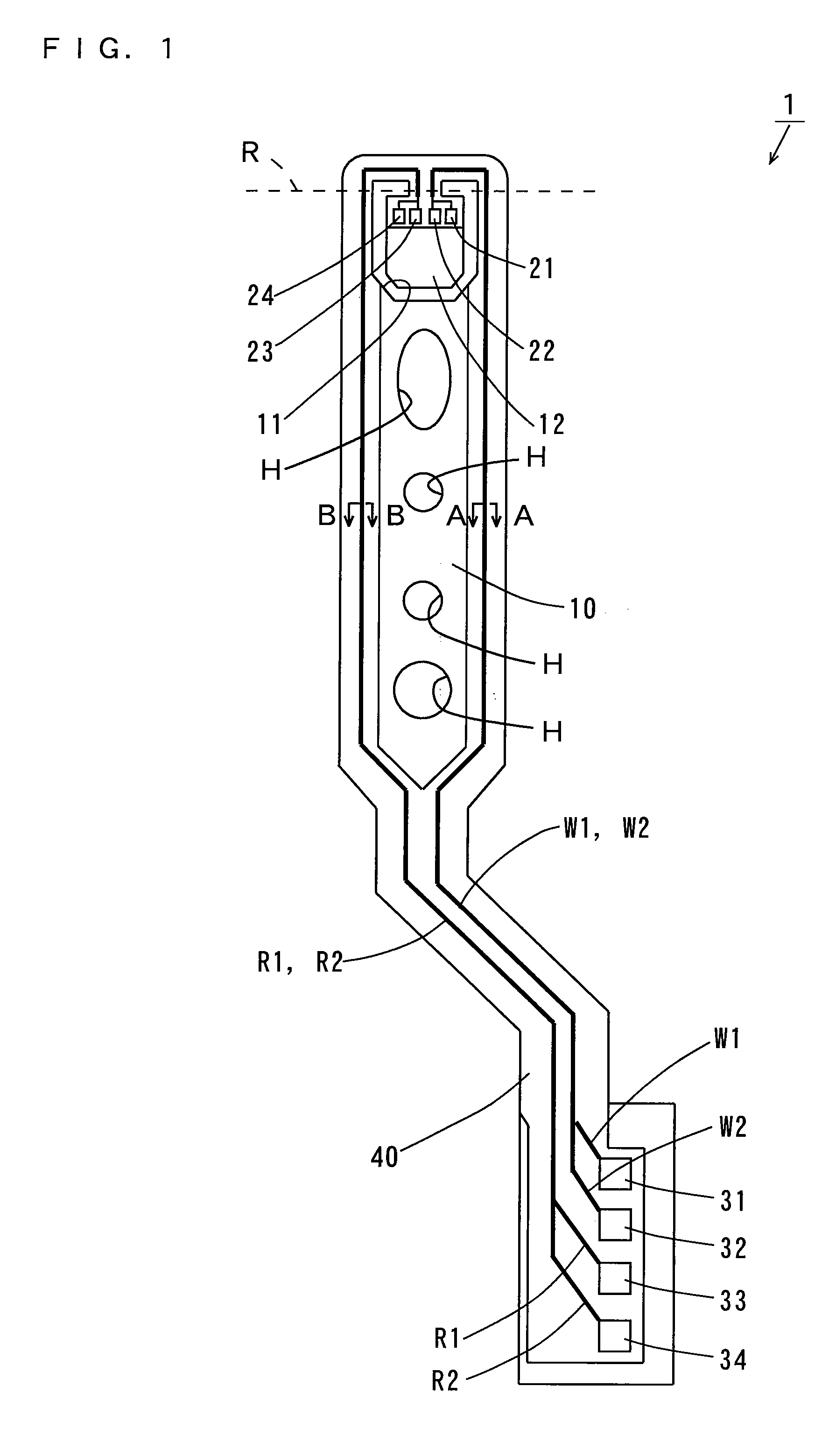
[0046]FIG. 1 is a top view of the suspension board according to a first embodiment of the present invention.
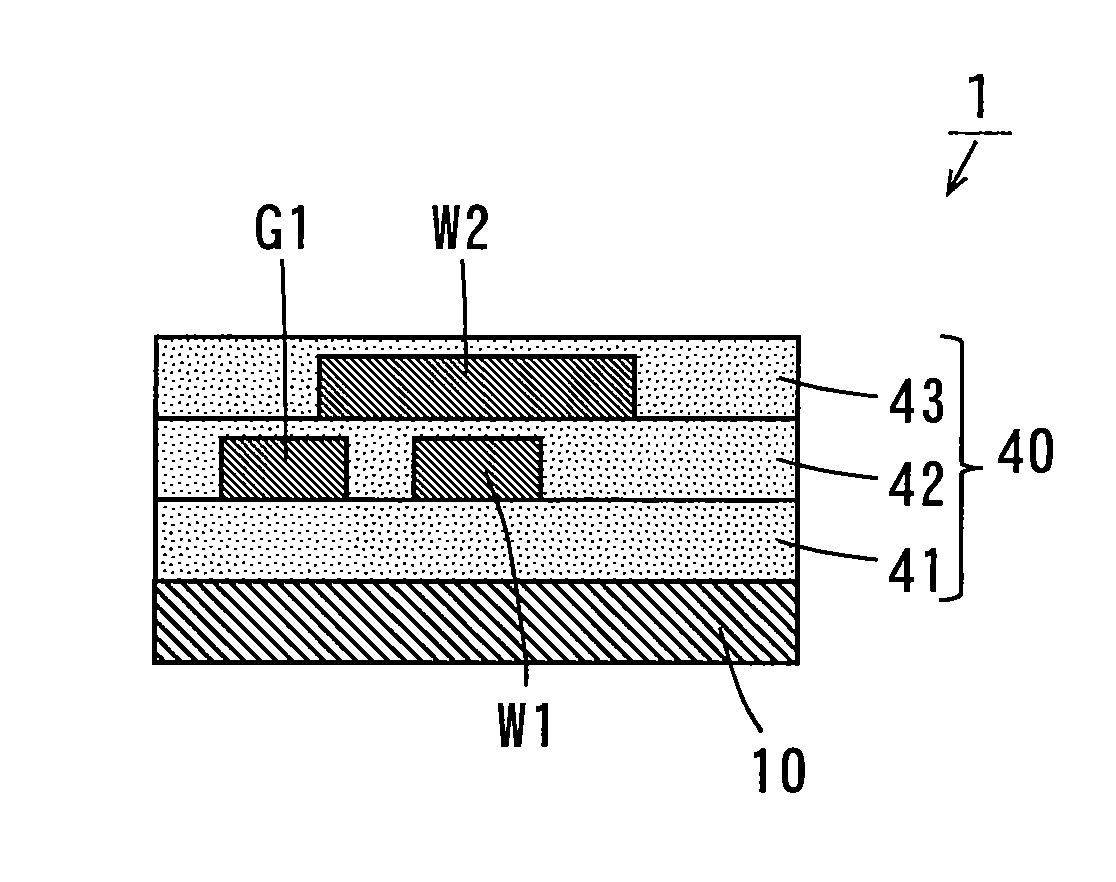
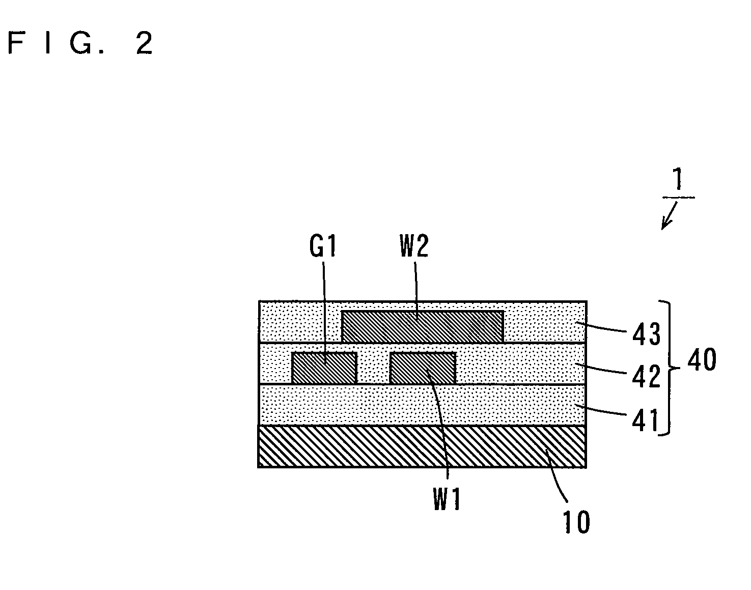
[0047]As shown in FIG. 1, the suspension board 1 includes a suspension body 10 formed of a long-sized metal substrate. Write wiring traces W1, W2 for writing information in a magnetic disk that is not shown and the read wiring traces R1, R2 for reading information from the magnetic disk are formed on the suspension body 10, as indicated by the bold solid lines.
[0048]At an end of the suspension body 10, a U-shaped opening 11 is formed, thereby providing a magnetic head supporting portion (hereinafter referred to as a tongue) 12. The tongue 12 is bent along the broken line R to form a predetermined angle with respect to the suspension body 10. Four electrode pads 21, 22, 23, 24 are formed at an end of the tongue 12.
[0049]Four electrode pads 31, 32, 33, 34 are formed at the other end of the suspension body 10. The electrode pads 21 t...
second embodiment
[0087]FIG. 5 is a vertical sectional view showing a suspension board according to a second embodiment of the present invention.
[0088]The suspension board 2 according to the present embodiment is different from the suspension board 1 of FIG. 2 in the following points.
[0089]As shown in FIG. 5, the ground trace G1 is formed on one side of the write wiring trace W1, and a ground trace G2 is formed on the other side of the write wiring trace W1 on the first insulating layer 41 in the present embodiment. The ground trace G2 is formed in the same manner as the ground trace G1.
[0090]Note that the width s5 of the ground trace G2 is set the same as the width s2 (FIG. 3(b)) of the ground trace G1. The spacing d2 between the write wiring trace W1 and the ground trace G2 is set the same as the spacing d1 of FIG. 3(b). The thickness t7 of the ground trace G2 is set the same as the thickness t3 of FIG. 3(b). The width s6 of a region, which is opposite to the ground trace G2, of the write wiring tr...
third embodiment
[0092]FIG. 6 is a vertical sectional view showing a suspension board according to a third embodiment of the present invention.
[0093]The suspension board 3 according to the present embodiment is different from the suspension board 2 of FIG. 5 in the following points.
[0094]As shown in FIG. 6, a ground trace G3 is formed on one side of the write wiring trace W2 while a ground trace G4 is formed on the other side of the write wiring trace W2 on the second insulating layer 42 in the present embodiment. The ground traces G3, G4 are formed in the same manner as the ground trace G1.
[0095]Note that each of the widths s7, s8 of the ground traces G3, G4 is not less than 5 μm and not more than 40 μm, and preferably not less than 10 μm and not more than 30 μm. The thickness t8 of each of the ground traces G3, G4 is set the same as the thickness t5 of FIG. 4(d). Each of the spacing d3 between the ground trace G3 and the write wiring trace W2 and the spacing d4 between the ground trace G4 and the ...
PUM
 Abstract
Description
Claims
Application Information
 - R&D
- Intellectual Property
- Life Sciences
- Materials
- Tech Scout
- Unparalleled Data Quality
- Higher Quality Content
- 60% Fewer Hallucinations
Browse by: Latest US Patents, China's latest patents, Technical Efficacy Thesaurus, Application Domain, Technology Topic, Popular Technical Reports.
© 2025 PatSnap. All rights reserved.Legal|Privacy policy|Modern Slavery Act Transparency Statement|Sitemap|About US| Contact US: help@patsnap.com


