Display apparatus and electronic equipment

a technology of electronic equipment and display apparatus, which is applied in the field of active matrix display apparatus, can solve the problems of large demerit of display apparatus concerning electric potential appearance and luminance sinking, and achieve the effect of reducing audio noise and improving the response speed of liquid crystal cells

Inactive Publication Date: 2012-11-13
JAPAN DISPLAY INC
View PDF9 Cites 3 Cited by
  • Summary
  • Abstract
  • Description
  • Claims
  • Application Information

AI Technical Summary

Benefits of technology

[0016]The capacitive coupling driving method is characterized that, in comparison with the 1H Vcom inversion driving method, the capacitive coupling driving method is capable of improving the response speed of the liquid-crystal cell due to the so-called overdrive, reducing audio noises generated in the frequency band of the common voltage signal Vcom and compensating the contrast for an ultra high definition display panel.

Problems solved by technology

If the capacitive coupling driving method disclosed in Patent document 3 is adopted in a liquid-crystal display apparatus employing liquid-crystal cells made of a liquid-crystal material having a characteristic like the one shown in FIG. 3, however, the display apparatus will introduce a big demerit concerning an electric potential appearing in the display pixel circuit.
The demerit is a problem of big luminance variations due to liquid-crystal gap variations / gate oxidation film thickness variations caused by manufacturing process variations or due to liquid-crystal cell relative dielectric constant variations caused by environment temperature variations.
In addition, an effort to optimize the black luminance faces a problem of the white luminance becoming black, that is, a problem of the white luminance sinking.

Method used


Image

  • Display apparatus and electronic equipment
  • Display apparatus and electronic equipment
  • Display apparatus and electronic equipment

Examples


Embodiment Construction

[0088]Preferred embodiments of the present invention are explained in detail by referring to diagrams as follows.

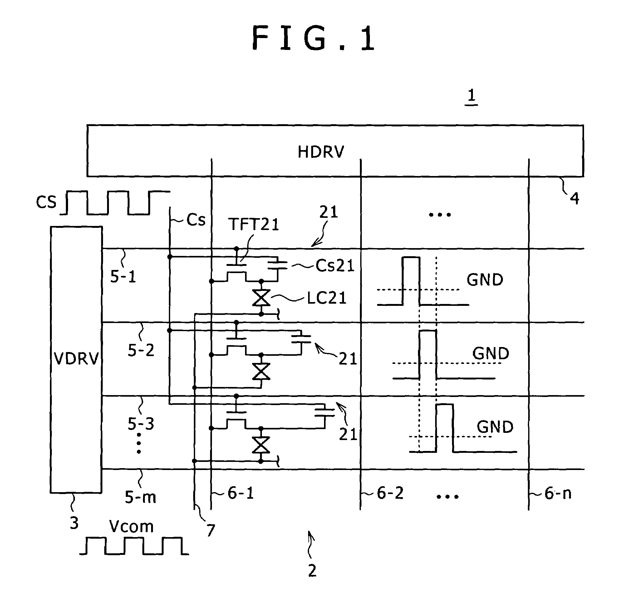
[0089]FIG. 4 is a diagram showing a typical configuration of an active-matrix display apparatus 100 implemented by an embodiment of the present invention as a display apparatus employing typically a liquid-crystal cell as a display element (also referred to as an electro optical device) in each pixel circuit. FIG. 5 is a circuit diagram showing a typical concrete configuration of an available pixel section 101 of the active-matrix display apparatus 100 shown in the diagram of FIG. 4.

[0090]As shown in FIGS. 4 and 5, the active-matrix display apparatus 100 has main components including the available pixel section 101, a vertical driving circuit (V / CSDRV) 102, a horizontal driving circuit (HDRV) 103, gate lines (each also referred to as a scan line) 104-1 to 104-m, capacitor lines (each also referred to as a storage line) 105-1 to 105-m, signal lines 106-1 to 106-n, a first ...


PUM


Abstract

Disclosed herein is a display apparatus including: an available pixel section; a plurality of scan lines; a plurality of capacitor lines; a plurality of signal lines; a driving circuit; a monitor circuit having a first monitor pixel section and a second monitor pixel section; at least two of following three correction systems of a capacitor-signal correction system, a video-signal correction system and the second monitor pixel section, and a common-voltage correction system; and a switch for selectively supplying pixel electric potentials detected by the first monitor pixel section and the second monitor pixel section to a desired one of the two or three correction systems.

Description

CROSS REFERENCES TO RELATED APPLICATIONS[0001]The present invention contains subject matter related to Japanese Patent Application JP 2007-224922 filed in the Japan Patent Office on Aug. 30, 2007, the entire contents of which being incorporated herein by reference.BACKGROUND OF THE INVENTION[0002]1. Field of the Invention[0003]The present invention relates to an active-matrix display apparatus employing pixel circuits arranged to form a matrix on the display area of the display apparatus as pixel circuits each having a display element also referred to as an electro-optical device and relates to electronic equipment including the display apparatus.[0004]2. Description of the Related Art[0005]By virtue of merits offered by a display apparatus as characteristics including a small thickness and a low power consumption, a display apparatus is employed widely in various kinds of electronic equipment including a PDA (Personal Digital Assistant), a hand-held phone, a digital camera, a video...

Claims


Application Information

Patent Timeline
Patent Type & Authority Patents(United States)
IPC IPC(8): G09G5/00
CPCG09G3/3655H04N5/70G09G3/3614G09G2300/0408G09G2300/0417G09G2300/0876G09G2320/0214G09G2320/0219G09G2320/029G09G2330/12G09G2320/0204G02F1/133G09G3/20G09G3/36
Inventor TOYOSHIMA, YOSHIHIKOITAKURA, NAOYUKIFUKANO, TOMOYUKI
Owner JAPAN DISPLAY INC
Why Eureka
Try Eureka