Dual inline lead-type electronic-part-mounted printed circuit board, method of soldering dual inline lead-type electronic part, printed circuit board and air-conditioner

a technology of electronic parts and printed circuit boards, which is applied in the direction of printed circuit components, printed circuit construction, electrical apparatus construction details, etc., can solve the problems of increased production costs, difficult to maintain soldering accuracy, and the shape of the slit does not substantially suppress the force of solder to be backed during soldering, so as to prevent the generation of solder bridges and solder chips. , the effect of improving the effect of soldering

Active Publication Date: 2012-11-13
MITSUBISHI ELECTRIC CORP
View PDF14 Cites 0 Cited by
  • Summary
  • Abstract
  • Description
  • Claims
  • Application Information

AI Technical Summary

Benefits of technology

[0012]In the above first patent document, furthermore, the rectangular solder-drawing land has a complicated shape provided with the lattice surface and smooth surface, and hence causes an increase in production cost. In addition, there is a need of increasing the size of the lattice surface and intervals of the lattice space to cause a sufficient solder-drawing effect, particularly a sufficient effect of suppressing the force of solder to be backed during soldering (i.e., the force of solder once drawn in the solder-drawing land to move back to the rearmost portion of the soldering land by the action of surface interfacial tension). In the above second patent document, the square solder-drawing land has a cross-shaped slit in the inside thereof. However, the cross-shaped slit does not substantially suppress the force of solder to be backed during soldering. Furthermore, in the case of the triangular solder-drawing land as illustrated in the above third patent document, it is more difficult to suppress the force of solder to be backed during soldering.
[0013]The present invention has been made in view of the above facts. Accordingly, it is an object of the present invention to provide a printed circuit board having a simplified geometry of a solder-drawing land. That is, when a dual inline lead-type electronic part is soldered to the board by jet-type soldering, such a simplified geometry of a solder-drawing land improves an effect of solder drawing and reliably prevents the generation of solder bridges and solder chips while preventing the occurrence of defects of soldering, particularly even in the case of soldering the dual inline lead-type electronic part with a narrow pitch between leads.
[0015]Since the printed circuit board mounted with a dual inline lead-type electronic-part according to the present invention is constructed as described above, the shape of a solder-drawing land is simplified to improve an effect of solder-drawing. Specifically, the surface / interfacial tension of the solder once drawn on the solder-drawing land can be dispersed by the slit. Therefore, there is an advantage of substantially preventing the generation of solder bridges and solder chips.

Problems solved by technology

However, the narrower the pitch of the leads in the longitudinal direction becomes or the narrower the distance between dual lines becomes, the more defects of soldering tends to occur, when lead-free solder with low solderability is used, Thus, it is difficult to maintain accuracy of soldering.
In the above first patent document, furthermore, the rectangular solder-drawing land has a complicated shape provided with the lattice surface and smooth surface, and hence causes an increase in production cost.
However, the cross-shaped slit does not substantially suppress the force of solder to be backed during soldering.
Furthermore, in the case of the triangular solder-drawing land as illustrated in the above third patent document, it is more difficult to suppress the force of solder to be backed during soldering.

Method used


Image

  • Dual inline lead-type electronic-part-mounted printed circuit board, method of soldering dual inline lead-type electronic part, printed circuit board and air-conditioner
  • Dual inline lead-type electronic-part-mounted printed circuit board, method of soldering dual inline lead-type electronic part, printed circuit board and air-conditioner
  • Dual inline lead-type electronic-part-mounted printed circuit board, method of soldering dual inline lead-type electronic part, printed circuit board and air-conditioner

Examples


embodiment 1

[0022]Referring now to FIG. 1 to FIG. 4, a printed circuit board mounted with a dual inline lead-type electronic-part according to Embodiment 1 of the invention will be described.

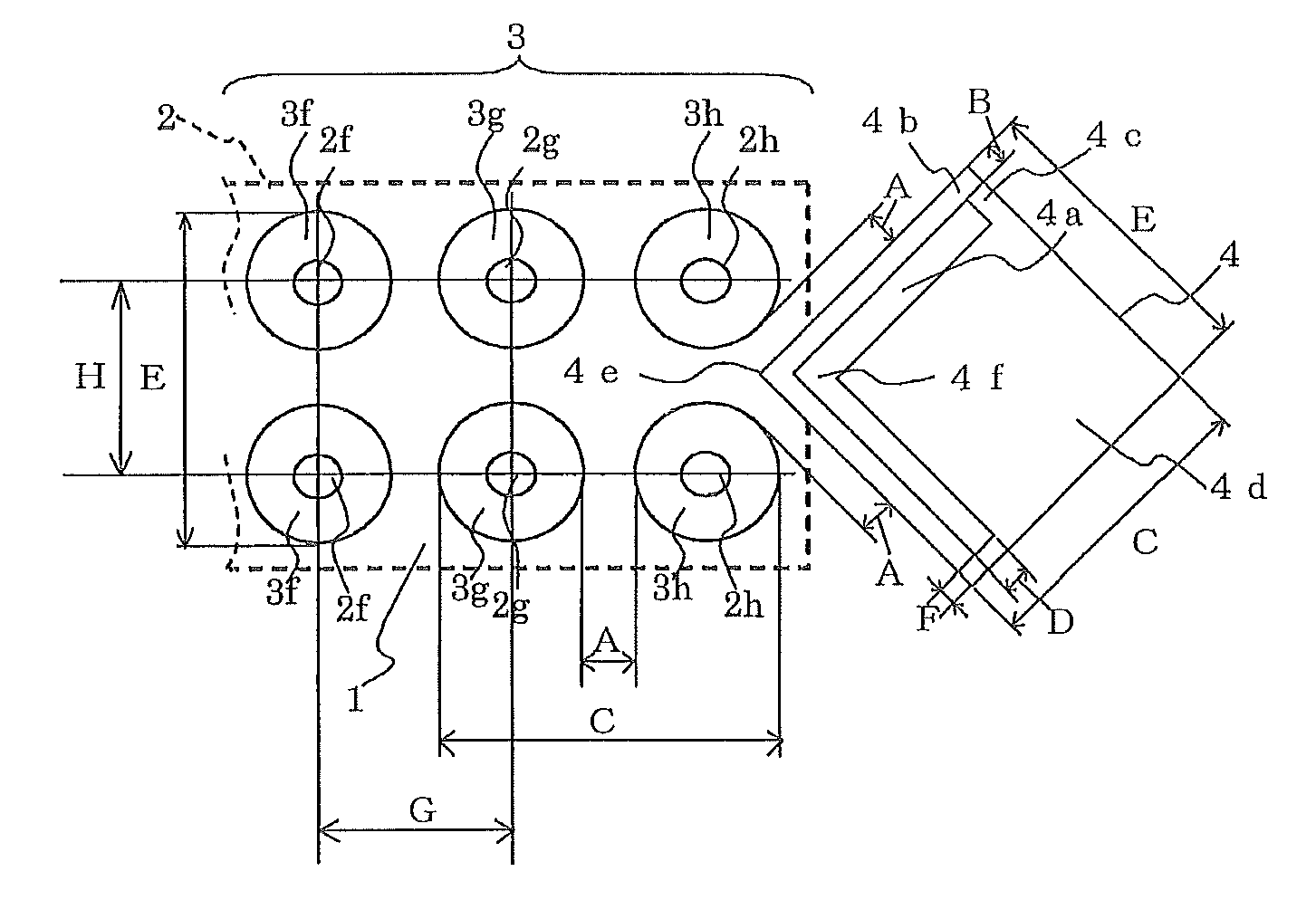
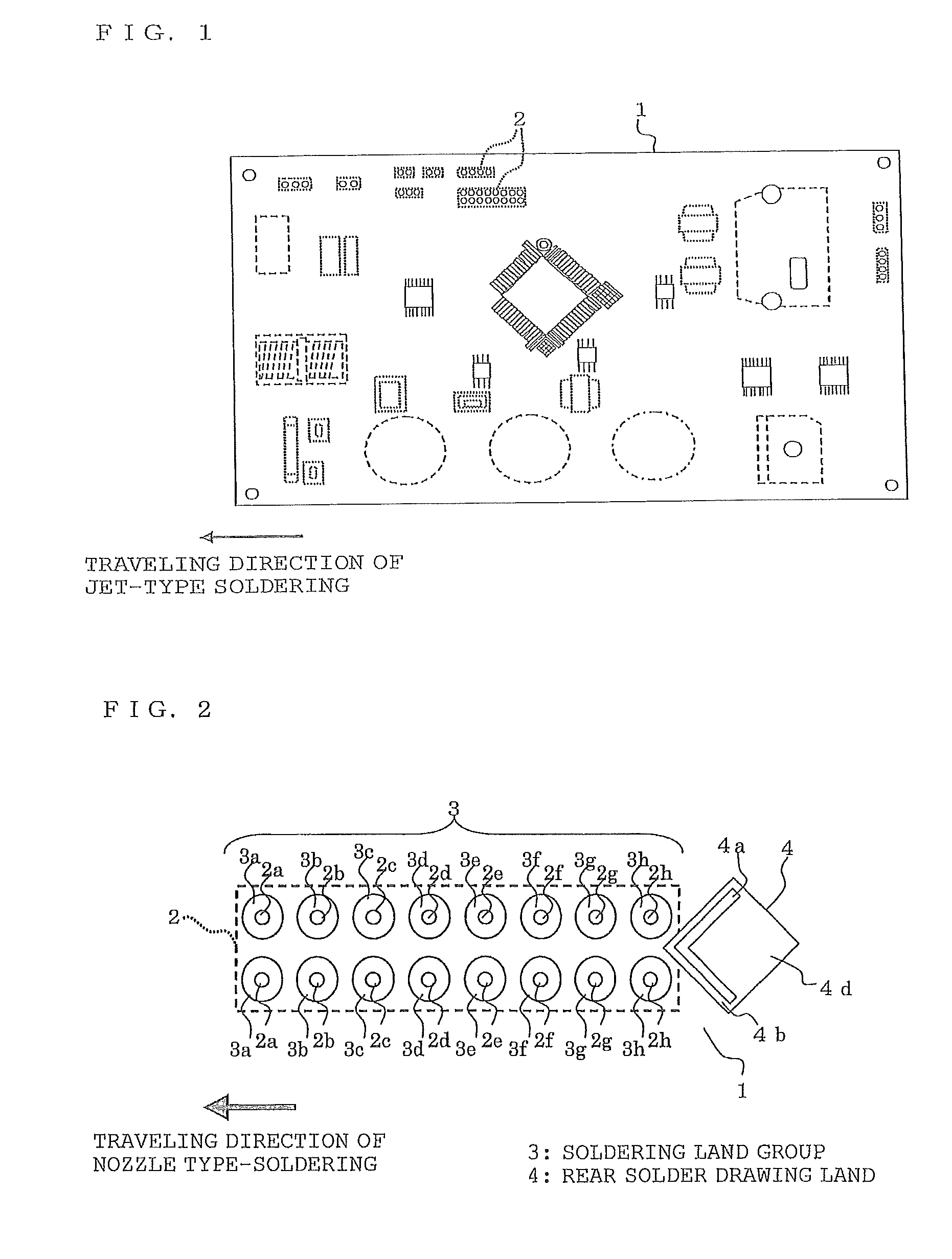
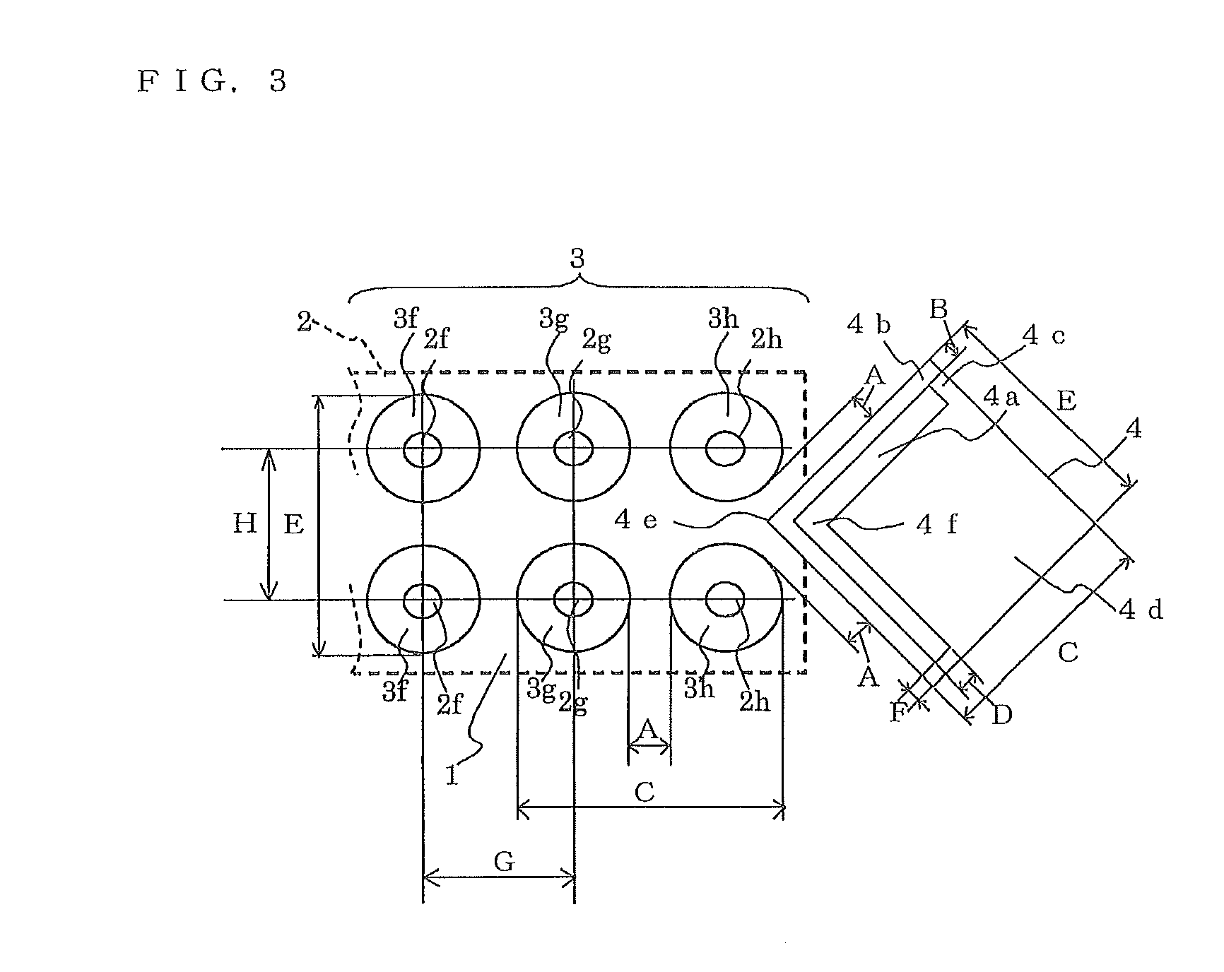
[0023]FIG. 1 is a schematic plan view of the configuration of a printed circuit board mounted with a dual inline lead-type electronic-part according to Embodiment 1 of the invention when viewed from the backside thereof. FIG. 2 is an enlarged plan view illustrating the arrangement relationship between a soldering land group of a dual inline lead-type electronic part and a solder-drawing land on the backside of the printed circuit board illustrated in FIG. 1. FIG. 3 is an enlarged plan view illustrating the dimensional relationship between the soldering lands on the rearmost position of the dual inline lead-type electronic part and the solder-drawing land illustrated in FIG. 2. FIG. 4 is a flowchart showing a process of jet-type soldering operation for soldering the dual inline lead-type electronic part to a...


PUM

PropertyMeasurementUnit
distanceaaaaaaaaaa
widthaaaaaaaaaa
widthaaaaaaaaaa

Abstract

A printed circuit board 1 is provided, which includes: soldering lands for connecting respective leads of a dual inline lead-type electronic part 2 by jet-type soldering; and a solder-drawing land 4 for absorbing excessive solder during soldering, which is arranged at a position behind the rearmost soldering lands 3h in the traveling direction of jet-type soldering. The solder-drawing land has a square outer shape and includes a slit 4a in a bent shape therein. One corner of the square is located near the rearmost soldering lands 3h and arranged between the leads, while a bent portion of the slit is arranged near the one corner.

Description

BACKGROUND OF THE INVENTION[0001]1. Field of the Invention[0002]The present invention relates to a printed circuit board on which a dual inline lead-type electronic part having a plurality of leads is mounted by jet-type soldering using a jet-type solder bath.[0003]2. Description of the Related Art[0004]In general, for a printed circuit board, it has been increasingly required to improve a packing density of parts thereon or miniaturize parts thereon. Therefore, dual inline lead-type electronic parts with narrow pitches or the like have been required to be mounted on the board. On the other hand, practical application of lead-free solder considering environmental problems becomes urgent necessity. However, the lead-free solder is inferior in solderability in comparison with leaded eutectic solder which has been conventionally used. Thus, short circuit at soldered portions between lead terminals of the dual inline lead-type electronic part or the like (referred to as solder bridge) h...

Claims


Application Information

Patent Timeline
Patent Type & Authority Patents(United States)
IPC IPC(8): H05K1/11H05K7/00H05K1/14H05K3/34
CPCH05K1/116H05K3/3468H05K3/3447Y10T29/49149H05K2201/10189H05K2203/046H05K2201/09781
Inventor MIURA, TSUYOSHI
Owner MITSUBISHI ELECTRIC CORP
Why Eureka
Try Eureka