Semiconductor device including metal silicide layer and method for manufacturing the same

a technology of metal silicide layer and semiconductor device, which is applied in the direction of semiconductor device, semiconductor/solid-state device details, electrical apparatus, etc., can solve the problems of difficult, if not impossible, to properly deposit refractory metal, and insufficient thickness of refractory metal layer, so as to reduce manufacturing time and cost, reduce manufacturing steps, and increase manufacturing efficiency

Active Publication Date: 2012-11-06
SAMSUNG ELECTRONICS CO LTD
View PDF15 Cites 13 Cited by
  • Summary
  • Abstract
  • Description
  • Claims
  • Application Information

AI Technical Summary

Benefits of technology

[0013]An aspect of the inventive concept provides a method of fabricating a fine metal silicide layer having a uniform thickness regardless of substrate doping. Another aspect of the inventive concept provides a method of fabricating a semiconductor device (e.g., field effect transistor) including a metal silicide layer, using fewer steps and thus increasing manufacturing efficiency and reducing manufacturing time and cost. Other aspects of the inventive concept provide memory chips and memory modules, CMOS imaging chips, nonvolatile memory cards, solid state drives (SSDs) and computing systems including a fine metal silicide layer formed on a silicon substrate.

Problems solved by technology

Moreover, the titanium easily reduces natural oxide unavoidably covering the contact area.
It is difficult, if not impossible, to properly deposit refractory metal on the bottom surface of a miniature contact hole having a large aspect ratio through a metal sputtering technique.
On the other hand, if the other refractory metal layer is optimized, the refractory metal layer is too thick, and material is wasted and leakage current may be increased.

Method used


Image

  • Semiconductor device including metal silicide layer and method for manufacturing the same
  • Semiconductor device including metal silicide layer and method for manufacturing the same
  • Semiconductor device including metal silicide layer and method for manufacturing the same

Examples


Embodiment Construction

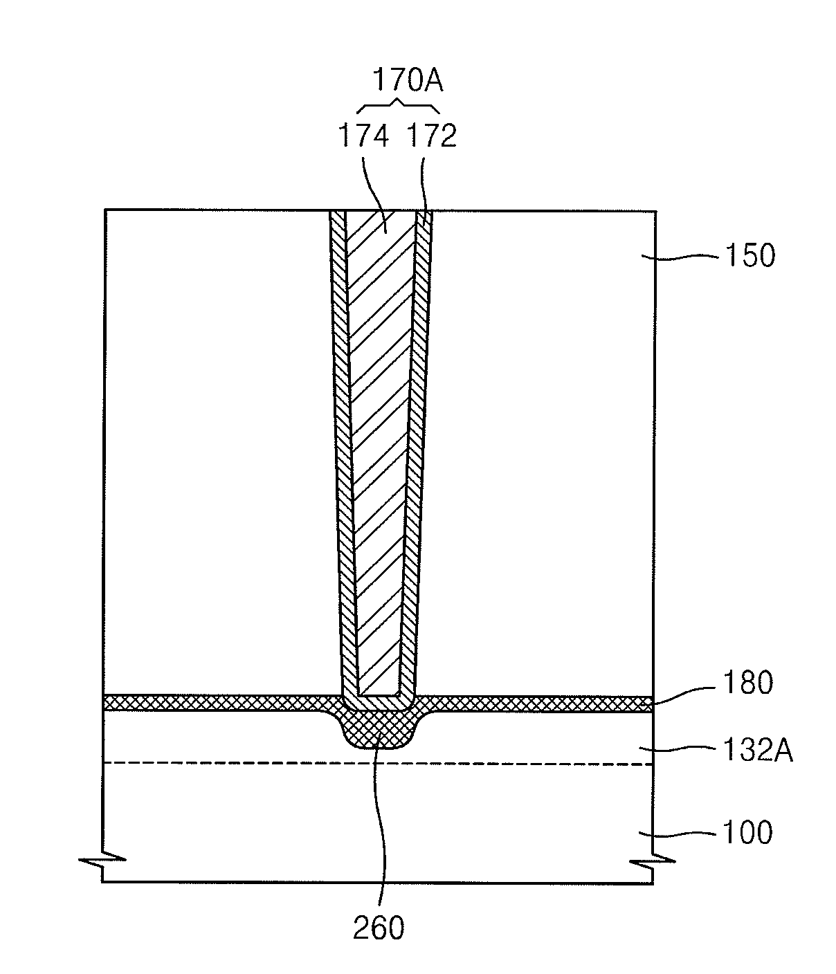
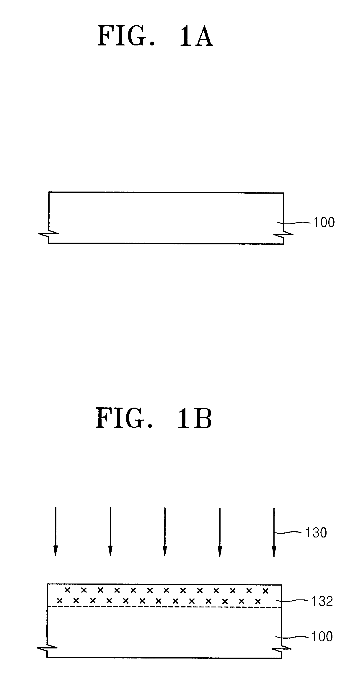
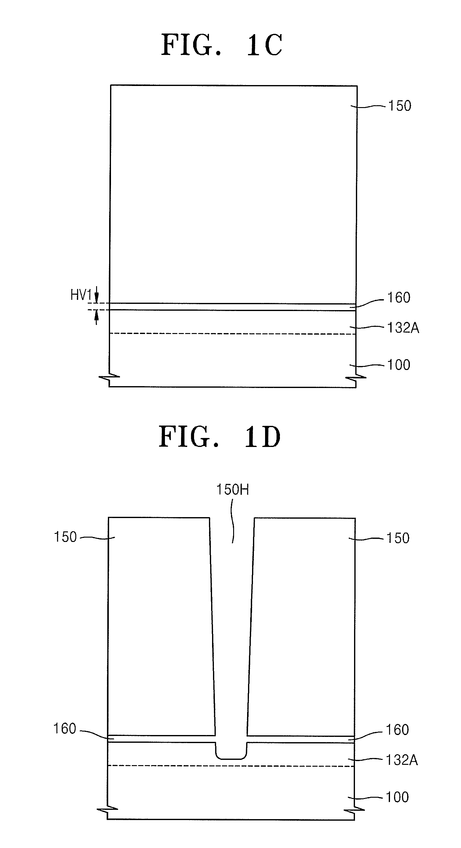
[0050]FIGS. 1a to 1f are cross sectional views showing a fabrication method of a semiconductor device including a metal silicide layer 180 and conductive plug 170A, according to a first exemplary embodiment of the inventive concept.

[0051]Referring to FIG. 1a, a silicon substrate 100, for example, a conventional single crystal silicon substrate of a first conduction type, is provided. In alternative embodiments, a semiconductor substrate 100 may be an epitaxial growth silicon layer formed on a non-semiconductor substrate (e.g., silicon on insulator, SOI). The first conduction type may be a p-type or n-type. For convenience of illustration, this disclosure illustrates an example process of using a p-type semiconductor substrate 100. Device isolation (e.g., trench isolation, e.g., shallow trench isolation, STI, e.g., 1010 shown in FIG. 15c) are formed buried in the silicon substrate 100 to define at least one active region in the semiconductor substrate 100. In various embodiments of t...


PUM

PropertyMeasurementUnit
temperatureaaaaaaaaaa
bias poweraaaaaaaaaa

Abstract

A device formed from a method of fabricating a fine metal silicide layer having a uniform thickness regardless of substrate doping. A planar vacancy is created by the separation of an amorphousized surface layer of a silicon substrate from an insulating layer, a metal source enters the vacancy through a contact hole through the insulating layer connecting with the vacancy, and a heat treatment converts the metal in the vacancy into metal silicide. The separation is induced by converting the amorphous silicon into crystalline silicon.

Description

CROSS-REFERENCE TO RELATED APPLICATIONS[0001]This U.S. non-provisional patent application claims priority, under 35 U.S.C. §119, of Korean Patent Application No. P2009-0097746, filed on Oct. 14, 2009, the entire contents of which are hereby incorporated by reference.BACKGROUND[0002]1. Field of the Inventive Concept[0003]The present inventive concept relates to a semiconductor device including a metal silicide layer of uniform thickness and method for manufacturing the same.[0004]2. Description of the Related Art[0005]Integrated circuits formed on semiconductor materials implement microelectronic devices that are widely used in the design of digital logic circuits such as microprocessors and memory devices for products ranging from satellites to consumer electronics. Advances in semiconductor chip fabrication technology, including technology development and process improvement obtained through scaling for high speed and high integration density, have raised the performance of digital...

Claims


Application Information

Patent Timeline
Patent Type & Authority Patents(United States)
IPC IPC(8): H01L29/76
CPCH01L21/28512H01L21/28518H01L21/2855H01L21/28556H01L21/74H01L21/76805H01L21/76834H01L21/76843H01L29/7833H01L29/7843H01L29/41758H01L29/458H01L2924/0002H01L29/6656H01L29/6659H01L2924/00H01L21/28052H01L21/28061H01L21/32051
Inventor JUNG, JONG-KI
Owner SAMSUNG ELECTRONICS CO LTD
Why Eureka
Try Eureka