Semiconductor optical amplification module, optical matrix switching device, and drive circuit
a technology of semiconductor optical amplification and drive circuit, which is applied in the direction of optical elements, semiconductor lasers, instruments, etc., can solve the problems of high power consumption, inability to achieve high-speed optical switching, and increase the power consumption of the drive circuit, so as to achieve the effect of suppressing ringing without increasing power consumption or circuit size or inhibiting high-speed operation
- Summary
- Abstract
- Description
- Claims
- Application Information
AI Technical Summary
Benefits of technology
Problems solved by technology
Method used
Image

Examples
first embodiment
[0053]the present invention will now be described in detail with reference to the drawings.
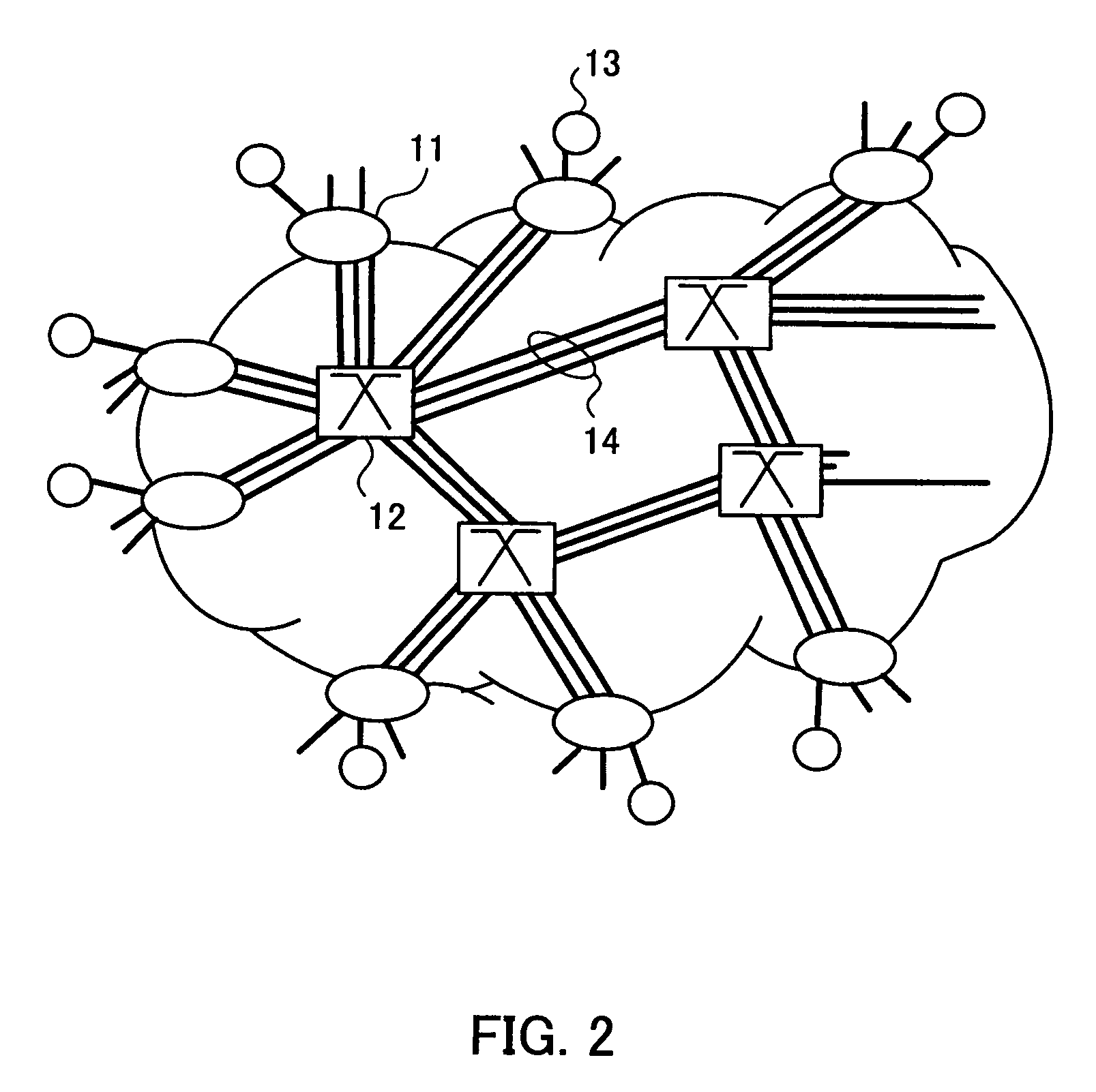
[0054]FIG. 2 is a view showing an example of the structure of an optical packet switching network to which an SOA module according to a first embodiment of the present invention is applied. As shown in FIG. 2, the optical packet switching network comprises edge nodes 11, core nodes 12, access nodes 13, and optical fibers 14.
[0055]The access node 13 such as a subscriber's terminal is connected to the edge node 11. The edge node 11 includes an optical packet assembly for converting signal data sent from the subscriber into an optical packet. In addition, the edge node 11 is connected to the core node 12.
[0056]The core node 12 switches the optical packet sent from the edge node 11 to another core node 12 or the edge node 11 under the control thereof.
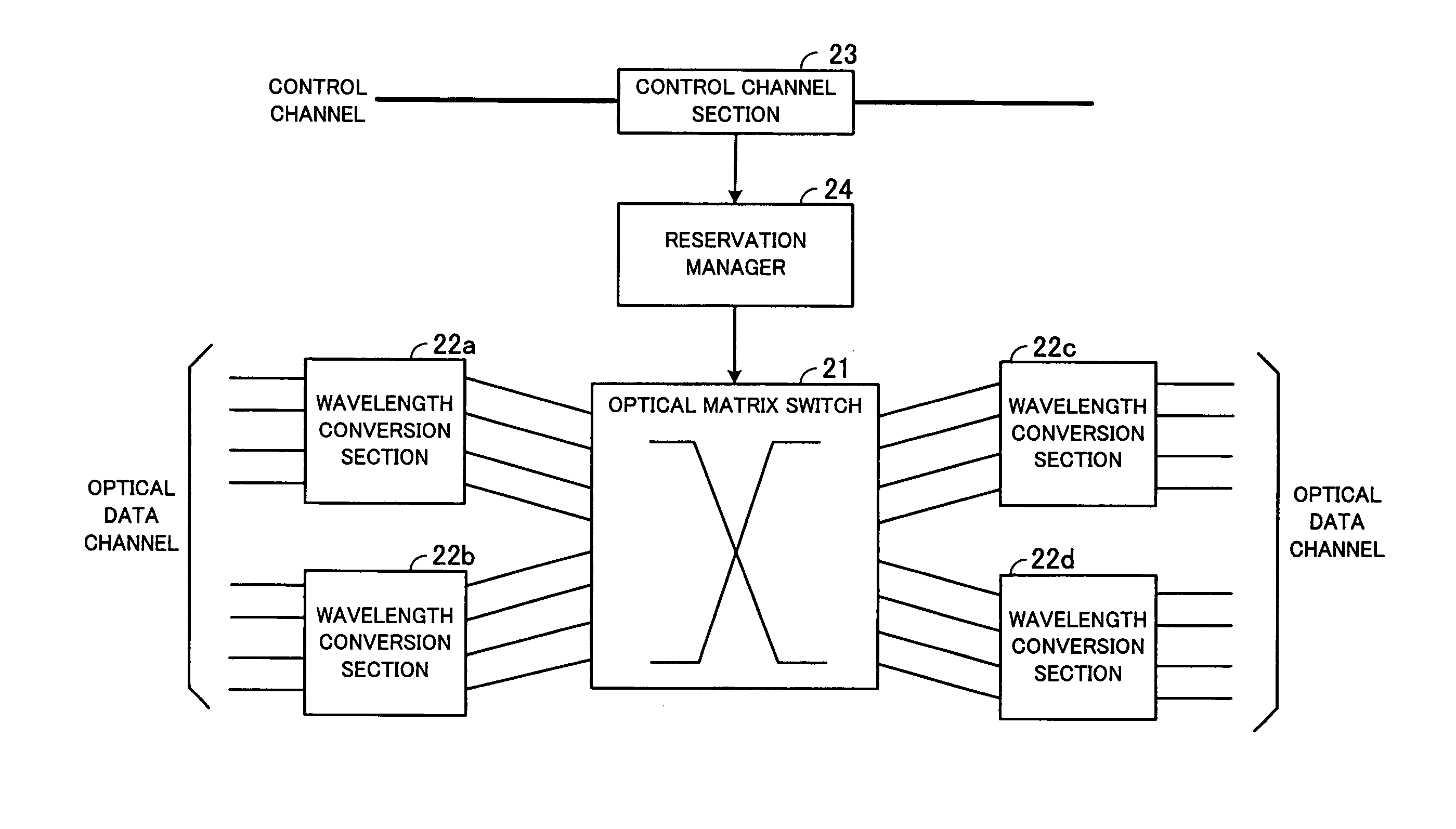
[0057]FIG. 3 is a view for describing the core node shown in FIG. 2. The core node 12 includes an optical matrix switch 21 for switching the optical ...
second embodiment
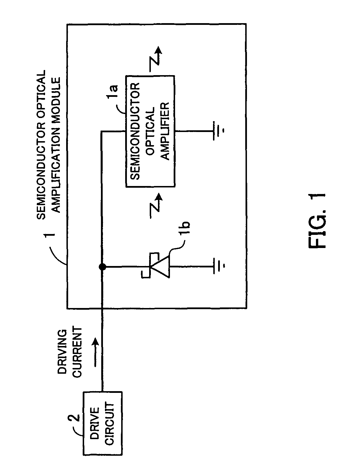
[0102]FIG. 12 is a view showing a drive circuit according to the present invention. Components in FIG. 12 that are the same as those shown in FIG. 10 are marked with the same symbols and descriptions of them will be omitted.
[0103]In FIG. 12, a Schottky barrier diode D2 included in an SOA module 62 is a GaAs Schottky barrier diode. An undershoot which appears on a negative side is suppressed by the GaAs Schottky barrier diode D2. This is the same with the silicon Schottky barrier diode D1 described in FIG. 10.
[0104]The junction capacitance of the GaAs Schottky barrier diode D2 is lower than that of a silicon Schottky barrier diode. Therefore, a response can be made at a higher speed and a great ringing suppression effect can be obtained.
[0105]FIG. 13 is a view for describing ringing of the circuit shown in FIG. 12. VSG shown in FIG. 13 indicates voltage at a point VSG shown in FIG. 12. VSOA shown in FIG. 13 indicates voltage at a point VSOA shown in FIG. 12. ISOA shown in FIG. 13 ind...
third embodiment
[0112]FIG. 14 is a view showing a drive circuit according to the present invention. Components in FIG. 14 that are the same as those shown in FIG. 10 are marked with the same symbols and descriptions of them will be omitted.
[0113]In FIG. 14, a Schottky barrier diode D3 and an SOA 51 are formed on one chip. That is to say, the Schottky barrier diode D3 and the SOA 51 are formed on the same wafer. The Schottky barrier diode D3 shown in FIG. 14 suppresses an undershoot which appears on a negative side. This is the same with the Schottky barrier diode D1 described in FIG. 10.
[0114]FIG. 15 is a view for describing ringing of the circuit shown in FIG. 14. VSG shown in FIG. 15 indicates voltage at a point VSG shown in FIG. 14. VSOA shown in FIG. 15 indicates voltage at a point VSOA shown in FIG. 14. ISOA shown in FIG. 15 indicates current at a point ISOA shown in FIG. 14. Each waveform shown in FIG. 15 indicates a result obtained by doing a simulation by the use of element values shown in ...
PUM
 Abstract
Description
Claims
Application Information
 - R&D
- Intellectual Property
- Life Sciences
- Materials
- Tech Scout
- Unparalleled Data Quality
- Higher Quality Content
- 60% Fewer Hallucinations
Browse by: Latest US Patents, China's latest patents, Technical Efficacy Thesaurus, Application Domain, Technology Topic, Popular Technical Reports.
© 2025 PatSnap. All rights reserved.Legal|Privacy policy|Modern Slavery Act Transparency Statement|Sitemap|About US| Contact US: help@patsnap.com