
Thin body semiconductor devices

a technology of thin body and semiconductors, applied in the field of thin body semiconductor devices, can solve problems such as the complexity of technology

Inactive Publication Date: 2012-09-11
GLOBALFOUNDRIES INC
View PDF4 Cites 7 Cited by
  • Summary
  • Abstract
  • Description
  • Claims
  • Application Information

AI Technical Summary

Benefits of technology

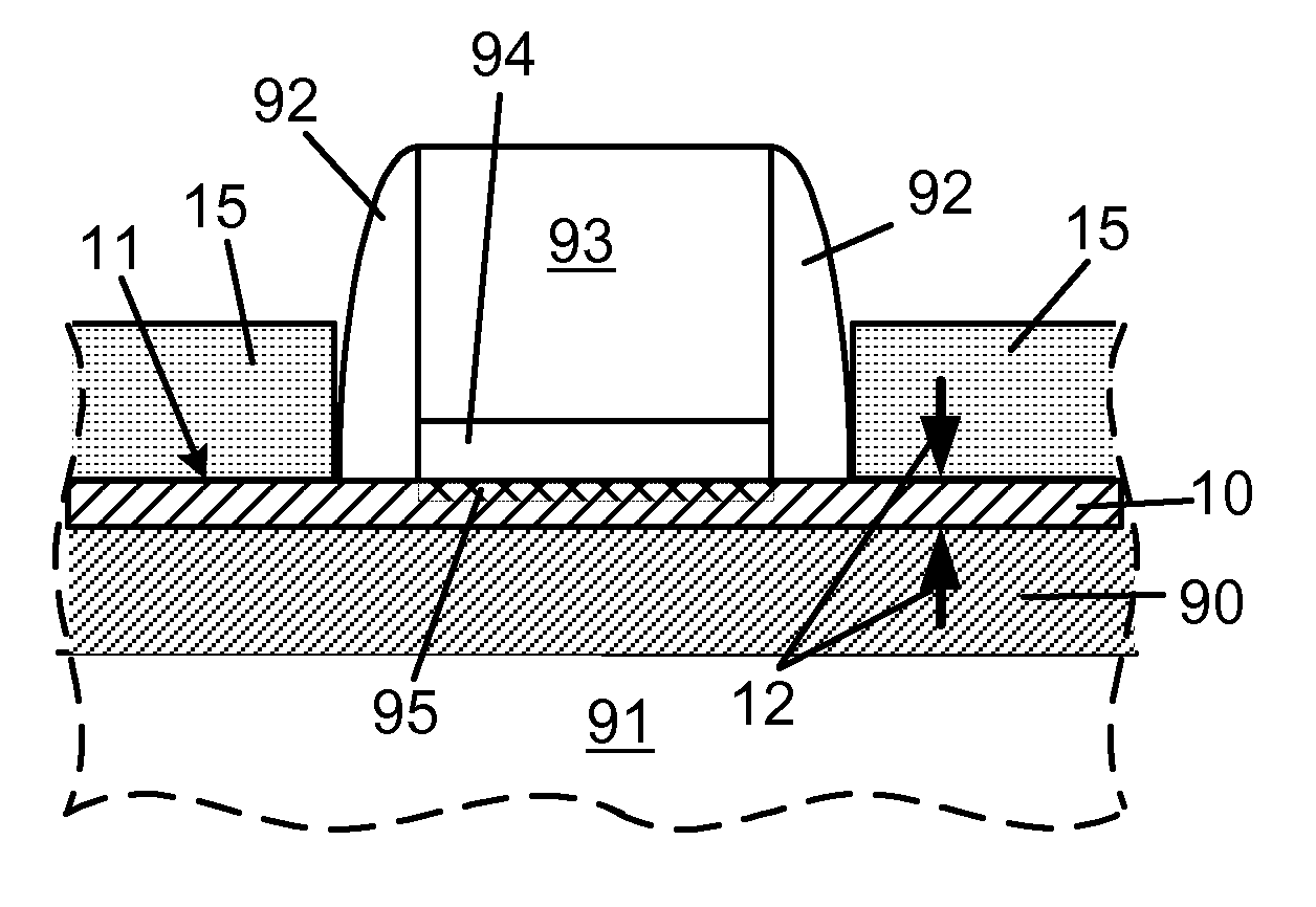
[0003]A method for fabricating an FET device is disclosed. The method includes providing a body over, and in direct contact with an insulator, with the body having at least one surface adapted to host a device channel. Selecting the body to be Si, Ge, or their alloy mixtures. Choosing the body layer to be less than a critical thickness defined as the thickness where agglomeration may set in during a high temperature processing. Such critical thickness may be about 4 nm for a planar devices, and about 8 nm for a non-planar devices. The method also involves clearing surfaces of oxygen at low temperature, and forming a raised source / drain by selective epitaxy using the cleared surfaces for seeding. The method further includes preventing oxygen exposure of the cleared surfaces after the clearing of the surfaces of oxygen and before the selective epitaxy.

Problems solved by technology

As FET (Field-Effect-Transistor) devices are being scaled down, the technology becomes more complex, and changes in device structures and new fabrication methods are needed to maintain the expected performance improvements from one successive device generation to the next.

Method used


Image

  • Thin body semiconductor devices
  • Thin body semiconductor devices
  • Thin body semiconductor devices

Examples


Embodiment Construction

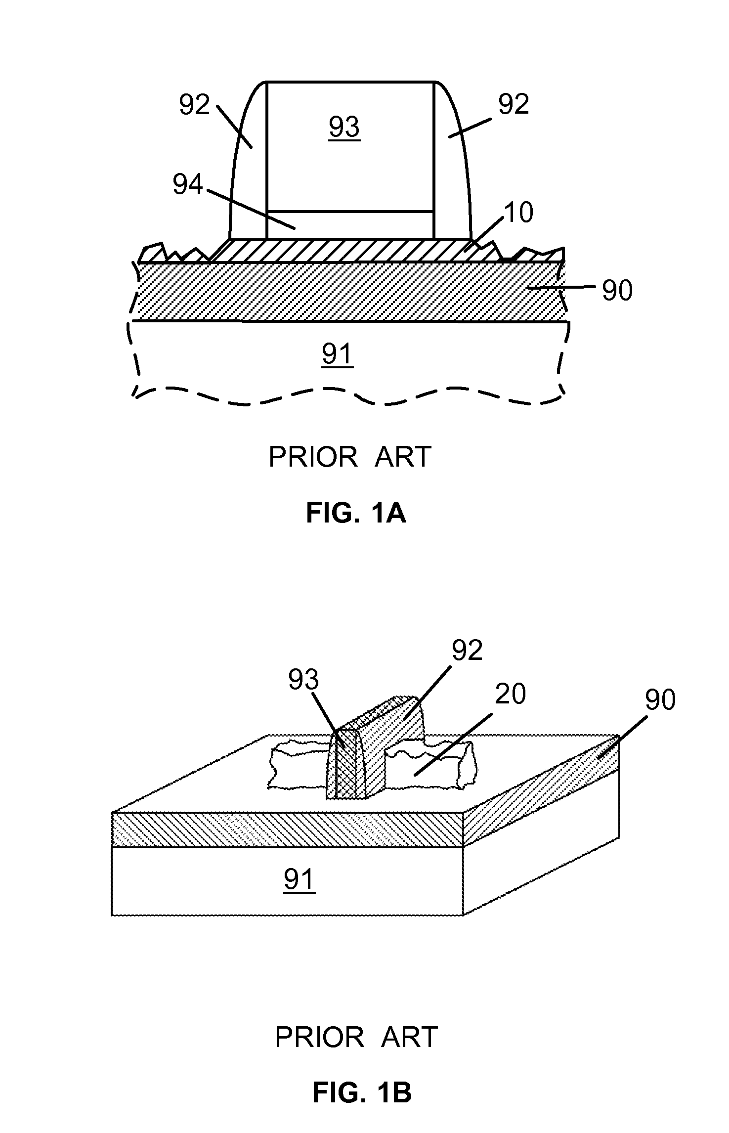
[0009]It is understood that FET (Field Effect Transistor) devices, often also referred as MOS devices, are well known in the electronic arts. Standard components of an FET are the source, the drain, the body in-between the source and the drain, and the gate. The gate is overlaying the body and is capable to induce a conducting channel on the surface of the body between the source and the drain. In the usual nomenclature, the body surface is adapted to host the channel. The gate is typically separated from the body by the gate insulator, or gate dielectric.

[0010]In general, FET devices may be planar devices, or non-planar devices. For planar FET devices the source, the drain, the channel are all associated with a single primary surface of a device body, which surface is without major curvatures or facets. The non-planar FET devices are three dimensional structures hosted by a fin structure. Hence, non-planar devices are often referred to in the art as FinFet devices. In FinFETs, the ...


PUM

PropertyMeasurementUnit
temperaturesaaaaaaaaaa
gate lengthaaaaaaaaaa

Abstract

A method for fabricating an FET device is disclosed. The method includes providing a body over an insulator, with the body having at least one surface adapted to host a device channel. Selecting the body to be Si, Ge, or their alloy mixtures. Choosing the body layer to be less than a critical thickness defined as the thickness where agglomeration may set in during a high temperature processing. Such critical thickness may be about 4 nm for a planar devices, and about 8 nm for a non-planar devices. The method further includes clearing surfaces of oxygen at low temperature, and forming a raised source / drain by selective epitaxy while using the cleared surfaces for seeding. After the clearing of the surfaces of oxygen, and before the selective epitaxy, oxygen exposure of the cleared surfaces is being prevented.

Description

BACKGROUND[0001]The present invention relates to electronic devices. In particular, it relates to SOI FET devices with body thicknesses in the few nanometers range.[0002]As FET (Field-Effect-Transistor) devices are being scaled down, the technology becomes more complex, and changes in device structures and new fabrication methods are needed to maintain the expected performance improvements from one successive device generation to the next. It is particular interest to make low resistivity ohmic contact to devices in the below 25 nm gate length range.BRIEF SUMMARY[0003]A method for fabricating an FET device is disclosed. The method includes providing a body over, and in direct contact with an insulator, with the body having at least one surface adapted to host a device channel. Selecting the body to be Si, Ge, or their alloy mixtures. Choosing the body layer to be less than a critical thickness defined as the thickness where agglomeration may set in during a high temperature processi...

Claims


Application Information

Patent Timeline
Patent Type & Authority Patents(United States)
IPC IPC(8): H01L21/336
CPCH01L29/66628H01L29/66742H01L29/66772H01L29/66795H01L29/78696
Inventor ADAM, THOMAS N.CHENG, KANGGUOKHAKIFIROOZ, ALIREZNICEK, ALEXANDERSADANA, DEVENDRA K.SHAHIDI, GHAVAM G.
Owner GLOBALFOUNDRIES INC
Learn More