
Functional paste

a technology of functional paste and antireflection layer, applied in the direction of electrically conductive paint, conductor, metal/alloy conductor, etc., can solve the problems of insufficient practical application, difficult method of direct patterning of antireflection layer, and complex method, and achieve good electrical properties

Inactive Publication Date: 2012-09-04
MERCK PATENT GMBH
View PDF19 Cites 9 Cited by
  • Summary
  • Abstract
  • Description
  • Claims
  • Application Information

AI Technical Summary

Benefits of technology

[0009]Inventors of the invention made extensive examinations to resolve the above issues, and found that during the fabrication process of paste by mixing a metal powder, a binder and an organic solvent, the mixture of an etching agent into the paste enables stable etching of an antireflection layer at a low temperature of approximately 200° C. in the fabrication of a surface electrode of a solar cell. The invention was achieved based on this finding.
[0026]According to the invention, an etching agent contained in the paste enables stable removal of an antireflection layer under a low temperature without penetrating the n-layer for the fabrication of electrodes of solar cells, thus achieving easy, single-step fabrication of surface electrodes with a low interface resistance.
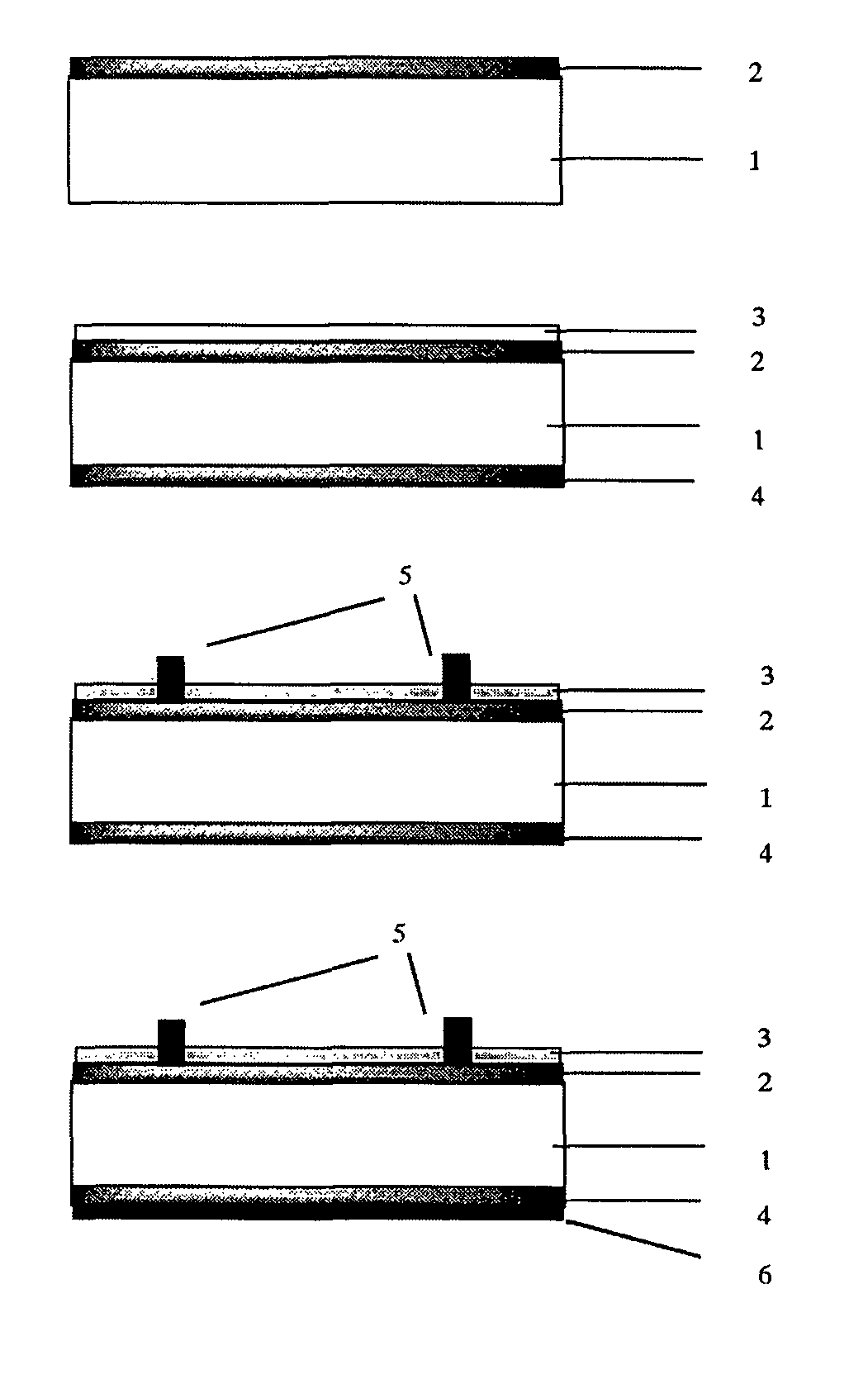
[0041]Then, after attachment and drying of the functional paste of the invention in a desired electrode shape using, e.g., a screen printing method, the paste is baked on the antireflection layer, so that a surface electrode which achieves good electric conduction with the n-layer silicon can be fabricated while etching the antireflection layer. The functional paste of the invention has both functions of the etching reaction for antireflection layers and the electric conduction; therefore, surface electrodes can be easily fabricated by a single step. Finally, by the formation of a back-surface electrode underneath the p+ layer, a solar cell with superior electrical properties can be obtained.

Problems solved by technology

However, this method is very complicated because it requires two steps: patterning of an antireflection layer, and fabrication of an electrode.
However, this method of direct patterning of antireflection layers has technological difficulties, and is not yet sufficient for practical application.
However, because this fire-through method requires a baking process generally at a high temperature of 850° C., the glass component and the electrode sometimes penetrate the n-layer, resulting in the deterioration of electrical properties of solar cells; therefore, accurate control of the fabrication conditions is necessary.
In addition, when there is no uniform conduction between the electrode and the n-layer silicon, initial electrical properties of solar cells deteriorate, leading to a problem.

Method used


Image

  • Functional paste

Examples


example 1

[0043]A mixture of[0044]Ag-coated Ni powder: 93 parts by weight (75.0 wt. %),[0045]oleic acid: 1 part by weight (0.8 wt. %),[0046]epoxy resin: 6 parts by weight (4.8 wt. %),[0047]ammonium hydrogen fluoride: 3 parts by weight (2.4 wt. %), and[0048]butyl carbitol: 6 parts by weight (4.8 wt. %),

prepared using a hybrid mixer was added with a mixture of glycerin / ethylene glycol=3 / 1 weight ratio in an amount of 15 parts by weight (12.1 wt. %), well mixed, and the resultant was applied on a Si wafer with a width approximately 1 mm, length approximately 1 cm, and thickness approximately 400 μm, then baked on a hot plate in air at 70-75° C. for 5 min and subsequently at 220° C. for 15 min, so that an electrode was formed. The resistance between the two electrodes was 90 Ω.

[0049]The preparation of the above composition excluding the ammonium hydrogen fluoride was used to form an electrode using the same process. The resistance between the two electrodes was 210 kΩ.

example 2

[0050]A mixture of[0051]Ag-coated Ni powder: 93 parts by weight (75.0 wt. %),[0052]oleic acid: 1 part by weight (0.8 wt. %),[0053]epoxy resin: 6 parts by weight (4.8 wt. %),[0054]ammonium hydrogen fluoride: 3 parts by weight (2.4 wt. %), and[0055]butyl carbitol: 6 parts by weight (4.8 wt. %),

prepared using a hybrid mixer was added with a mixture of glycerin / ethylene glycol=3 / 1 weight ratio in an amount of 15 parts by weight (12.1 wt. %), well mixed, and the resultant was applied on a Si wafer having a SiO2 layer of approximately 80 nm thickness, with a width approximately 1 mm, length approximately 1 cm, and thickness approximately 400 μm, then baked on a hot plate in air at 70-75° C. for 5 min and subsequently at 220° C. for 15 min, so that an electrode was formed. The resistance between the two electrodes was 900 Ω.

[0056]The preparation of the above composition excluding the ammonium hydrogen fluoride was used to form an electrode using the same process. The resistance between the...

example 3

[0057]A mixture of[0058]Ag-coated Ni powder: 93 parts by weight (66.9 wt. %),[0059]oleic acid: 1 part by weight (0.7 wt. %),[0060]epoxy resin: 6 parts by weight (4.3 wt. %),[0061]ammonium hydrogen fluoride: 3 parts by weight (2.2 wt. %), and[0062]butyl carbitol: 6 parts by weight (4.3 wt. %),

prepared using a hybrid mixer was added with a mixture of glycerin / ethylene glycol=3 / 1 weight ratio in an amount of 15 parts by weight (10.8 wt. %) and a silver colloidal solution AgE-102 (Nippon Paint Co., Ltd.) in an amount of 15 parts by weight (10.8 wt. %), well mixed, and the resultant was applied on a Si wafer having a SiO2 layer, with a width approximately 1 mm, length approximately 1 cm, and thickness approximately 400 μm, then baked on a hot plate in air at 70-75° C. for 5 min and subsequently at 220° C. for 15 min, so that an electrode was formed. The resistance between the two electrodes was 160 Ω.

[0063]The preparation of the above composition excluding the silver colloidal solution A...


PUM

PropertyMeasurementUnit
temperatureaaaaaaaaaa
viscosityaaaaaaaaaa

Abstract

To provide functional paste with etching activity and good electrical properties. Functional paste comprising a metal powder, an etching agent, a binder and an organic solvent.

Description

FIELD OF THE INVENTION[0001]The invention relates to functional paste having an etching function and conductivity.BACKGROUND OF THE INVENTION[0002]At present extensive research has been performed on conductive paste containing a metal powder, because it is used for various purposes including fabrication of electrodes for solar cells, formation of jamper cables using electronic components, e.g., printed-wiring boards, and formation of terminal outgoing lines of printed resistors.[0003]For example, in the fabrication of surface electrodes of solar cells, conventionally, an antireflection layer formed on a semiconductor layer is patterned using photoresist, then a surface electrode is fabricated (patent reference 1). However, this method is very complicated because it requires two steps: patterning of an antireflection layer, and fabrication of an electrode.[0004]To eliminate the patterning process of antireflection layers, a method was proposed, wherein an antireflection layer is form...

Claims


Application Information

Patent Timeline
Patent Type & Authority Patents(United States)
IPC IPC(8): H01B1/22H01L21/00B05D7/24C09D5/24C09D7/12C09D161/10C09D163/00C09D201/00C09K13/08H01L31/0224H05K1/09
CPCC09K13/08H01L31/022425H05K1/097Y02E10/50H05K1/095H01B1/22H01L31/04H01L31/0224
Inventor KLEIN, SYLKEKUEBELBECK, ARMINSTOCKUM, WERNERNAKANOWATARI, JUNKAWAMOTO, KIYOHIKOTANINO, KATSUMI
Owner MERCK PATENT GMBH
Learn More