
Method for manufacturing double gate finFET with asymmetric halo

a technology of asymmetric halo and double gate, which is applied in the direction of basic electric elements, electrical equipment, semiconductor devices, etc., can solve the problems of reducing the operating margin, reducing the size of the fet, so as to reduce the fet design to such a small size or operating margin, and achieves reduced capacitance and short channel effects without degrading the carrier mobility in the channel. , the effect o

Inactive Publication Date: 2012-07-24
GLOBALFOUNDRIES INC
View PDF22 Cites 9 Cited by
  • Summary
  • Abstract
  • Description
  • Claims
  • Application Information

AI Technical Summary

Benefits of technology

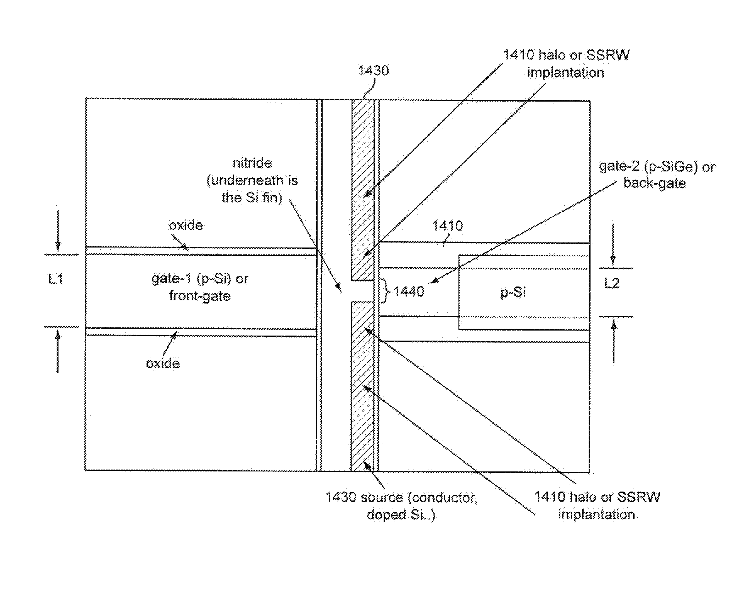
The present invention provides a finFET structure with reduced capacitance and short channel effects, while maintaining high carrier mobility in the channel. This is achieved by using a halo implant asymmetrically located in a channel of the finFET proximate to the second gate and forming a super-steep retrograde well for a conduction channel adjacent to and controlled by the first gate. The method of forming the finFET includes steps of forming a conduction channel as a fin, forming first and second gate structures on opposite sides of the fin, and performing an angled impurity implant as a halo implant adjacent the second gate structure forming a super-steep retrograde well for the conduction channel portion controlled by the first gate. This results in a simplified, economical, and repeatable method for manufacturing the finFET with high yield.

Problems solved by technology

However, some electrical characteristics of FETs may be degraded as FET designs are scaled to such extremely small sizes or operating margins may be reduced due to requirements of electrical breakdown, reduced voltages for thermal management and the like.
For example, switching threshold voltages may not be sufficiently uniform to allow reliable operations at current and foreseeable clock rates unless some control therefor is provided.
Unfortunately, a second gate is difficult to provide in a common planar FET design having, for example, a conduction channel in a substrate and a gate on the surface thereof.
This lower doping tends to compromise control of the switching threshold of finFETs.
Further, since finFETs are double gate devices, allowing the back gate to be used to adjust the switching threshold, Vt, the back gate also increases capacitance which tends to degrade finFET performance.
It is known that a so-called halo implant can be used to improve short channel effects but such structures, in a finFET, degrades carrier mobility in the channel.
Similarly, a super-steep retrograded well can reduce SCE but is very difficult to form the well for planar MOSFET designs.

Method used


Image

  • Method for manufacturing double gate finFET with asymmetric halo
  • Method for manufacturing double gate finFET with asymmetric halo
  • Method for manufacturing double gate finFET with asymmetric halo

Examples


Embodiment Construction

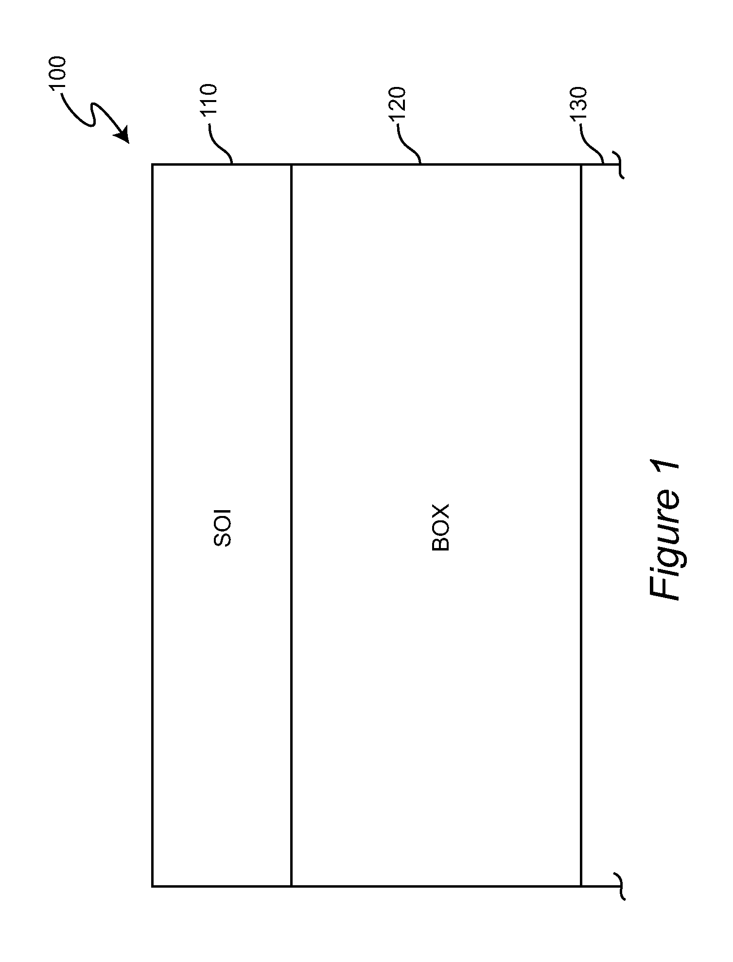
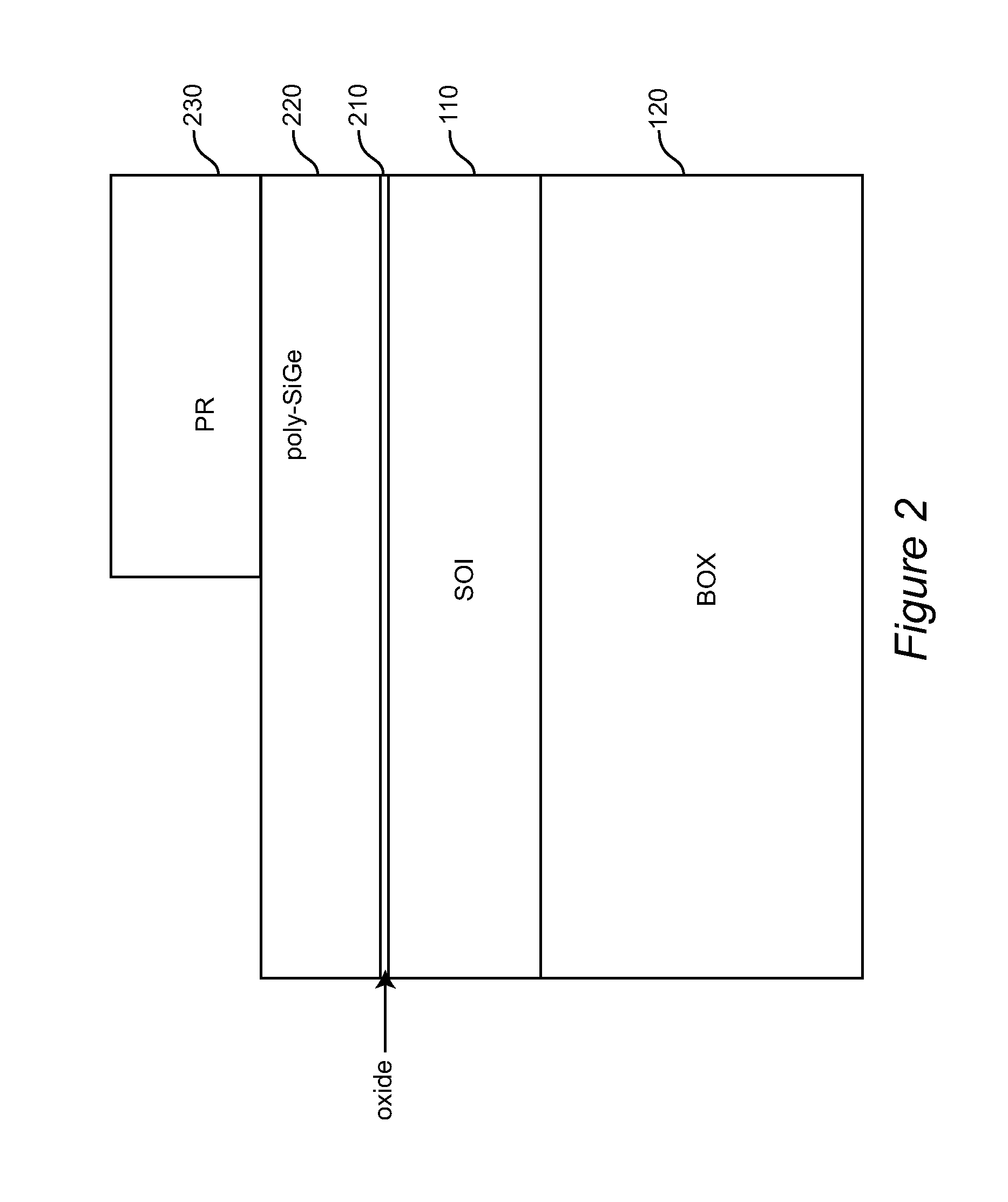
[0017]Referring now to the drawings, and more particularly to FIG. 1, there is shown in cross-sectional view, a portion of a semiconductor-on-insulator (SOI) wafer which is preferred for fabrication of finFETs in accordance with the invention. However, it is to be understood that the invention may be practiced using other materials and other types of wafers as will be understood by those skilled in the art in view of the following description of the invention. It should also be appreciated that the cross-sectional views of FIGS. 1-12, 16-21 and 23-26 are taken within the central region of the channel (e.g. section A-A) in such that the source and drain of the transistor are in front of in back of the plane of the page of each respective Figure. FIGS. 22 and 23 include a cross-section (e.g. section B-B) taken adjacent the conduction channel.

[0018]FIG. 1 illustrates the cross-section of an SOI wafer 100. As is known in the art, an SOI wafer is often preferred for current transistor de...


PUM


Abstract

A finFet controls conduction channel conditions using one of two gate structures, preferably having a gate length shorter than the other gate structure to limit capacitance, which are opposed across the conduction channel. An asymmetric halo impurity implant performed at an angle adjacent to the gate structure for controlling conduction channel conditions forms a super steep retrograde well to limit short channel effects in the portion of the conduction channel which is controlled by the other gate structure.

Description

BACKGROUND OF THE INVENTION[0001]1. Field of the Invention[0002]The present invention generally relates to field effect transistors (FETs) and, more particularly, to double gate FETs configured as finFETs.[0003]2. Description of the Prior Art[0004]Field effect transistors have become the device of choice for fabrication of integrated digital logic circuits operating at all but the highest of clock rates. FETs can be fabricated at extremely small sizes consistent with extremely small minimum feature size regimes. However, some electrical characteristics of FETs may be degraded as FET designs are scaled to such extremely small sizes or operating margins may be reduced due to requirements of electrical breakdown, reduced voltages for thermal management and the like. For example, switching threshold voltages may not be sufficiently uniform to allow reliable operations at current and foreseeable clock rates unless some control therefor is provided. One such control technique is to employ...

Claims


Application Information

Patent Timeline
Patent Type & Authority Patents(United States)
IPC IPC(8): H01L21/336
CPCH01L29/66795H01L29/785H01L29/78612H01L29/7855H01L29/7856
Inventor ZHU, HUILONGGLUSCHENKOV, OLEGWANG, JING
Owner GLOBALFOUNDRIES INC
Learn More