Semiconductor integrated circuit device

a technology of integrated circuit and semiconductor, applied in the direction of semiconductor devices, semiconductor/solid-state device details, electrical apparatus, etc., can solve the problems of increasing the occurrence of defective contacts, and achieve the effect of improving reliability and productivity

Inactive Publication Date: 2012-06-26
SAMSUNG ELECTRONICS CO LTD
View PDF45 Cites 2 Cited by
  • Summary
  • Abstract
  • Description
  • Claims
  • Application Information

AI Technical Summary

Benefits of technology

[0008]Aspects of the present invention provide a semiconductor integrated circuit device with improved reliability and productivity.

Problems solved by technology

However, a decrease in the size of the metal contacts makes it difficult to accurately pattern the metal contacts, resulting in an increase in the occurrence of defective contacts.

Method used


Image

  • Semiconductor integrated circuit device
  • Semiconductor integrated circuit device
  • Semiconductor integrated circuit device

Examples


Embodiment Construction

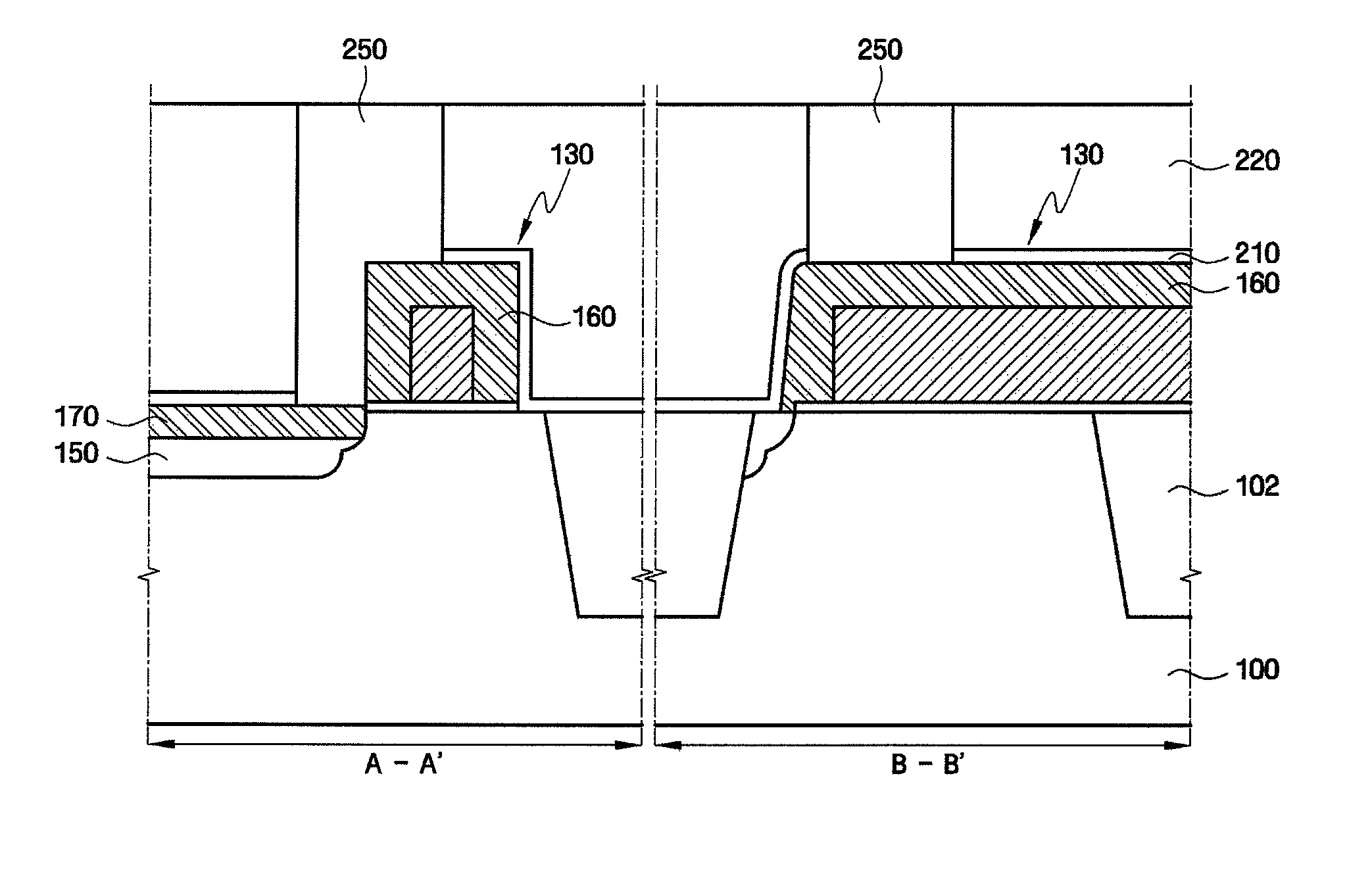
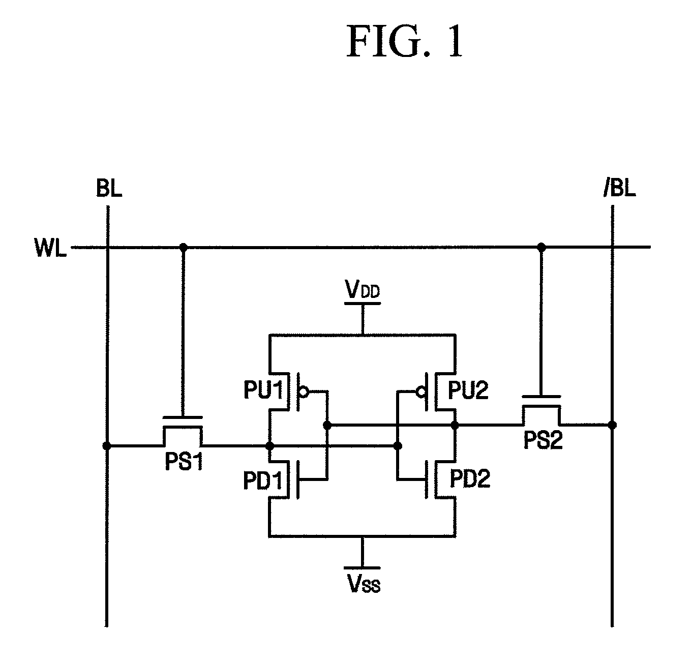
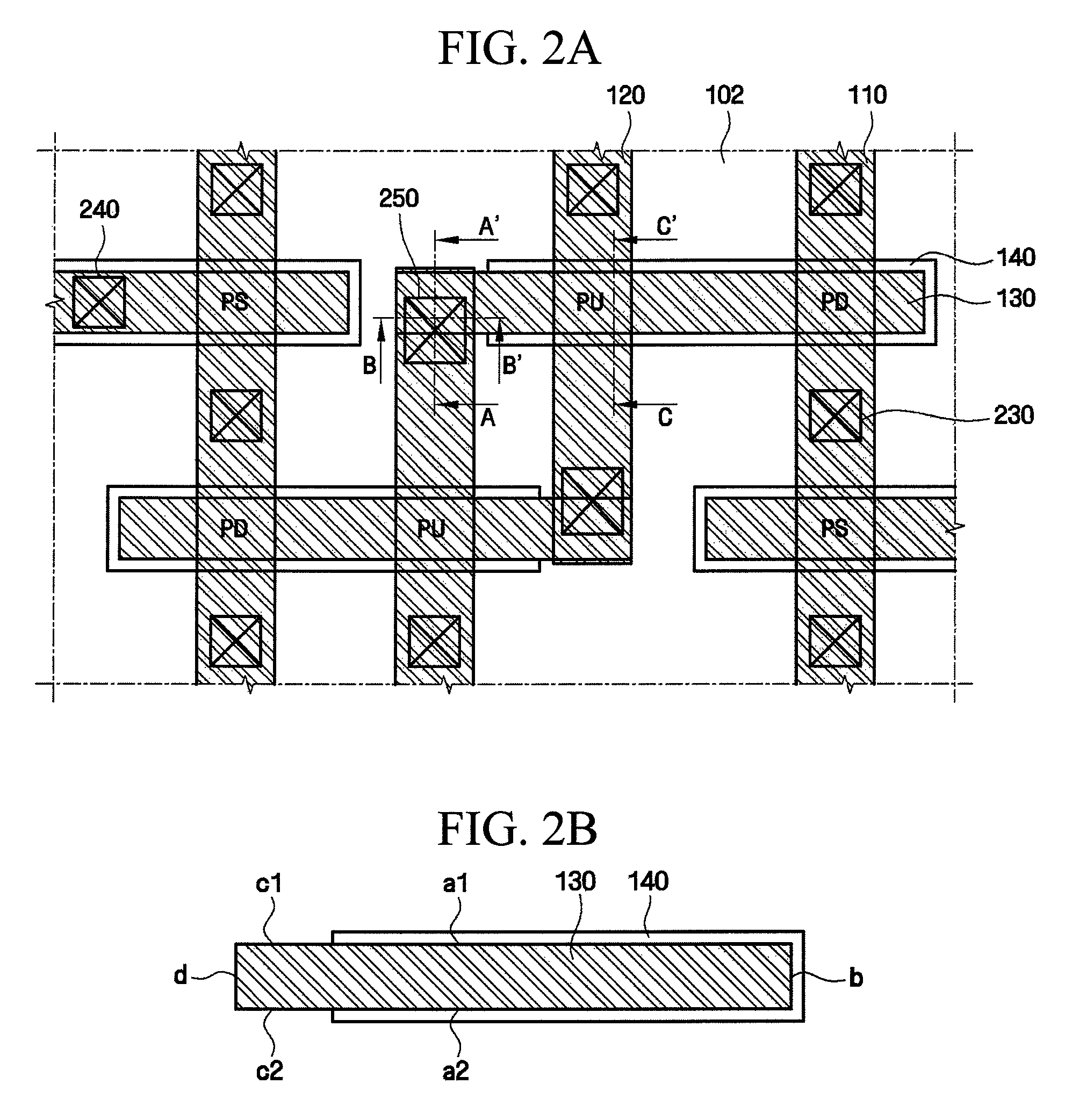
[0035]FIG. 1 is a circuit diagram of a static random access memory (SRAM) cell included in a semiconductor integrated circuit (IC) memory device according to exemplary embodiments of the present invention.

[0036]Referring to FIG. 1, the semiconductor integrated circuit device according to the exemplary embodiments includes a six-transistor SRAM cell. The SRAM cell includes a plurality of (e.g., two) pull-up transistors PU1 and PU2 and a plurality of (e.g., two) pull-down transistors PD1 and PD2 which constitute a latch and a plurality of (e.g., two) pass transistors PS1 and PS2 which access the latch.

[0037]Each SRAM memory cell includes first and second pass transistors PS1 and PS2, first and second pull-down transistors PD1 and PD2, and first and second pull-up transistors PU1 and PU2. The first and second pass transistors PS1 and PS2 and the first and second pull-down transistors PD1 and PD2 are n-channel metal oxide semiconductor (NMOS) transistors, and the first and second pull-u...


PUM


Abstract

A semiconductor integrated circuit memory device includes a gate line that extends in a first direction, an active region adjacent to a first end of the gate line and that extends in a second direction, a silicide layer formed on a top surface of the active region, on a top surface of the gate line, on both sidewalls of the first end of the gate line, and on a transverse endwall of the first end of the gate line. A spacer may be formed on sidewalls of the gate line, excluding the first end of the gate line, and a contact shared by the active region may be formed on the first end of the gate line.

Description

[0001]This application claims priority, under 35 U.S.C. §119, of Korean Patent Application No. 10-2009-0010238 filed on Feb. 9, 2009 in the Korean Intellectual Property Office, which is incorporated by reference herein in its entirety.BACKGROUND[0002]1. Field of the Invention[0003]The present invention relates to a semiconductor integrated circuit device, and more particularly, to a semiconductor integrated circuit (IC) memory device with enhanced reliability.[0004]2. Description of the Related Art[0005]Static random access memories (SRAMs) have a smaller memory capacity for a given chip area but a higher operating speed than dynamic random access memories (DRAMs). Accordingly, SRAMs are widely used in cache memories of computers or portable appliances that are required to operate at high speed.[0006]SRAM cells are divided into thin-layer transistor (TFT) cells and full complementary metal oxide semiconductor (FCMOS) cells. An FCMOS cell includes a plurality of cross-connected pull-...

Claims


Application Information

Patent Timeline
Patent Type & Authority Patents(United States)
IPC IPC(8): H01L29/40
CPCH01L27/11H01L27/1104H01L27/0207H10B10/00H10B10/12
Inventor SHIN, DONG SUKCHANG, CHONG-KWANG
Owner SAMSUNG ELECTRONICS CO LTD
Why Eureka
Try Eureka