
High electron mobility transistor and method for fabricating the same

a high-electromagnetic transistor and electron mobility technology, applied in the field of high-frequency devices, can solve the problems of insufficient effective mass, difficult epitaxy growth, complex composition of superlattice structure,

Active Publication Date: 2012-05-01
YLTLINK TECH CORP
View PDF3 Cites 98 Cited by
  • Summary
  • Abstract
  • Description
  • Claims
  • Application Information

AI Technical Summary

Benefits of technology

[0010]For the foregoing embodiments, the high electron mobility transistor and the method for fabricating the same can be applied not only to improve the high-frequency characteristics of the transistor (e.g. high current gain cut-off frequency, low noise figure), but also to be helpful for freeing the nanometer-scaled gate length of the high electron mobility transistor from having to be fabricated with an electron-beam lithography system when persons skilled in the art develop the transistor with high efficacy, such that the gate electrode can be defined by the optical lithography stepper so as to raise the yield rate.

Problems solved by technology

For a high electron mobility transistor (HEMT) as a high-frequency device, when a channel layer therein is grown by epitaxy and has a superlattice structure, the composition of the superlattice structure is usually complex and thus difficult to be grown by epitaxy.
On the contrary, if purer indium gallium arsenide (InGaAs) is used, for the HEMT having a hetero-structure, the indium (In) content therein may not be high enough so that in the HEMT the electron effective mass is not small enough and the electron mobility is inclined to be low.
As a result, the direct-current characteristics and high-frequency characteristics of the HEMT are not better.
However, if the nanometer-scaled gate length is fabricated in order to improve the device characteristics, the electron-beam lithography system has to be used.
Thus, the production cannot be raised and the production costs could increase.

Method used


Image

  • High electron mobility transistor and method for fabricating the same
  • High electron mobility transistor and method for fabricating the same
  • High electron mobility transistor and method for fabricating the same

Examples


Embodiment Construction

[0020]In the following description, several specific details are presented to provide a thorough understanding of the embodiments of the present invention. One skilled in the relevant art will recognize, however, that the present invention can be practiced without one or more of the specific details, or in combination with or with other components, etc. In other instances, well-known implementations or operations are not shown or described in detail to avoid obscuring aspects of various embodiments of the present invention.

[0021]The terms used in this specification generally have their ordinary meanings in the art and in the specific context where each term is used. The use of examples anywhere in this specification, including examples of any terms discussed herein, is illustrative only, and in no way limits the scope and meaning of the invention or of any exemplified term. Likewise, the present invention is not limited to various embodiments given in this specification.

[0022]As use...


PUM


Abstract

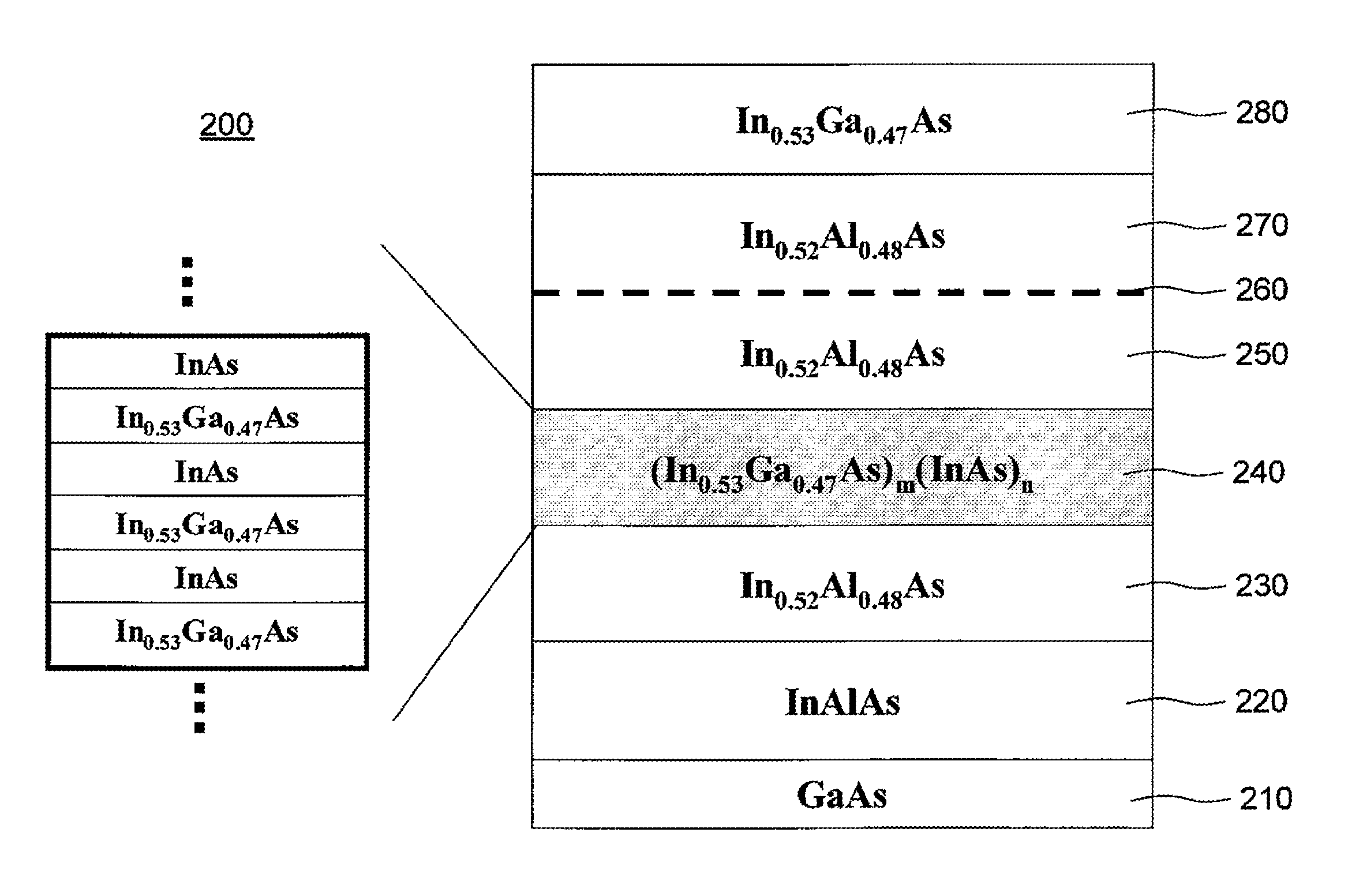
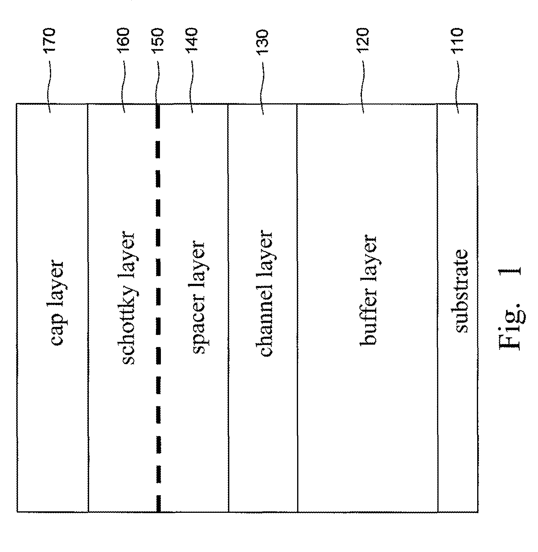
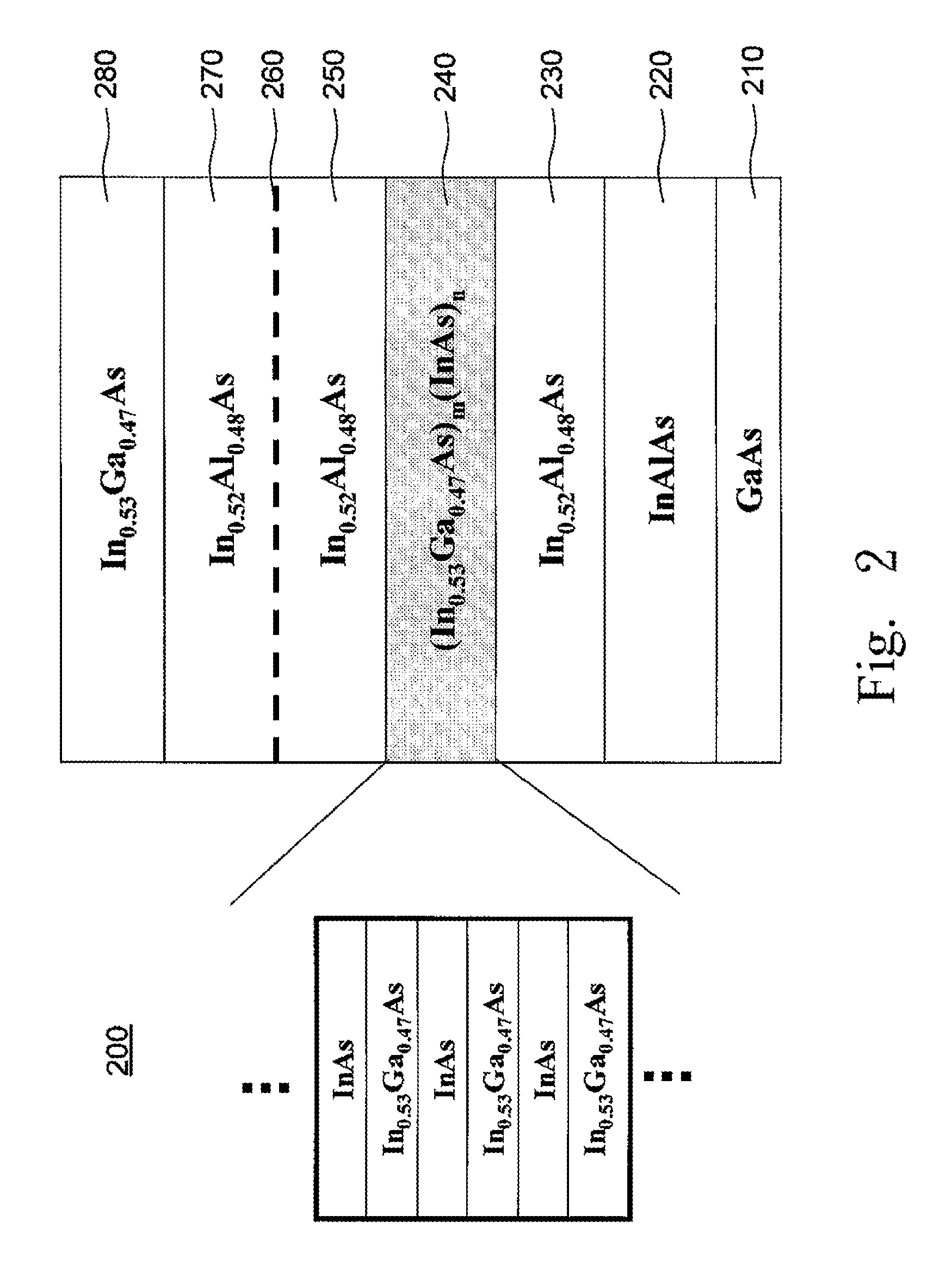
A high electron mobility transistor includes a substrate, a buffer layer, a channel layer, a spacer layer, a schottky layer and a cap layer. The buffer layer is formed on the substrate. The channel layer is formed on the buffer layer, in which the channel layer comprises a superlattice structure formed with a plurality of indium gallium arsenide thin films alternately stacked with a plurality of indium arsenide thin films. The spacer layer is formed on the channel layer. The schottky layer is formed on the spacer layer. The cap layer is formed on the schottky layer.

Description

RELATED APPLICATIONS[0001]This application claims priority to Taiwan Patent Application Serial Number 98146534, filed Dec. 31, 2009, which is herein incorporated by reference.BACKGROUND[0002]1. Technical Field[0003]The present disclosure relates to a high-frequency device. More particularly, the present disclosure relates to a high electron mobility transistor with a superlattice structure.[0004]2. Description of Related Art[0005]For a high electron mobility transistor (HEMT) as a high-frequency device, when a channel layer therein is grown by epitaxy and has a superlattice structure, the composition of the superlattice structure is usually complex and thus difficult to be grown by epitaxy. On the contrary, if purer indium gallium arsenide (InGaAs) is used, for the HEMT having a hetero-structure, the indium (In) content therein may not be high enough so that in the HEMT the electron effective mass is not small enough and the electron mobility is inclined to be low. As a result, the ...

Claims


Application Information

Patent Timeline
Patent Type & Authority Patents(United States)
IPC IPC(8): H01L29/66H01L21/338
CPCB82Y10/00H01L29/1029H01L29/15H01L29/66462H01L29/7783H01L29/7787
Inventor CHANG, EDWARD YIKUO, CHIEN-IHSU, HENG-TUNG
Owner YLTLINK TECH CORP
Learn More