
Capacitor triggered silicon controlled rectifier

a rectifier and capacitor technology, applied in the field of semiconductor devices, can solve the problems of contact spiking, silicon melting, or metal interconnection melting, and increase the susceptibility to electrostatic discharge damage (esd) damage,

Active Publication Date: 2012-03-06
CYPRESS SEMICON CORP
View PDF32 Cites 10 Cited by
  • Summary
  • Abstract
  • Description
  • Claims
  • Application Information

AI Technical Summary

Problems solved by technology

As integrated circuit (IC) geometries continue to shrink, susceptibility to electrostatic discharge (ESD) damage increases.
In particular, decreasing gate oxide thicknesses in MOS (metal-oxide-semiconductor) devices relative to breakdown voltage has resulted in an increased susceptibility to damage from the application of excessive voltages.
This charge transfer can develop voltages that are large enough to break down insulating gate oxides, leading to failures, such as contact spiking, silicon melting, or metal interconnect melting.
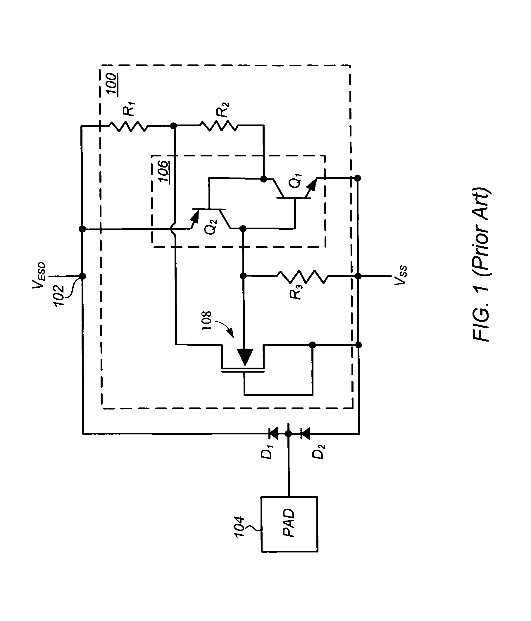
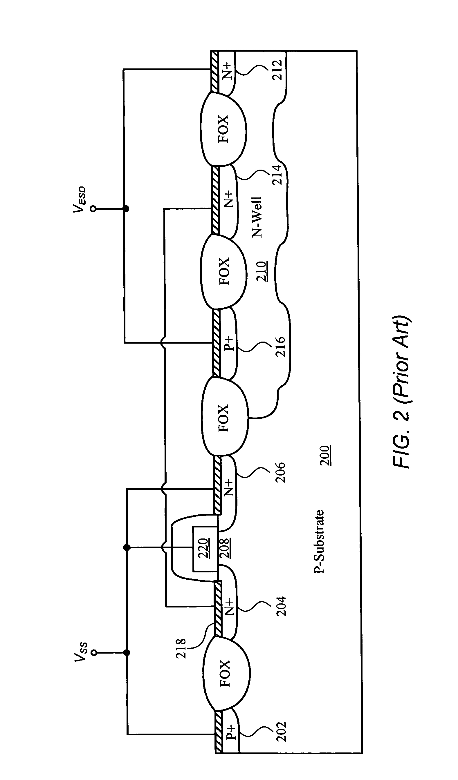
Thus, the turn on characteristic of the protection circuit is too slow for devices using technologies less than 65 nm, and in particular for fast ESD events, such as those described by the Charged Device Model (CDM) failures.
In addition, conventional protection circuits such as in FIG. 1 have a trigger voltage that can be high enough to cause damage in thin gate dielectrics that need to be protected.

Method used


Image

  • Capacitor triggered silicon controlled rectifier
  • Capacitor triggered silicon controlled rectifier
  • Capacitor triggered silicon controlled rectifier

Examples


Embodiment Construction

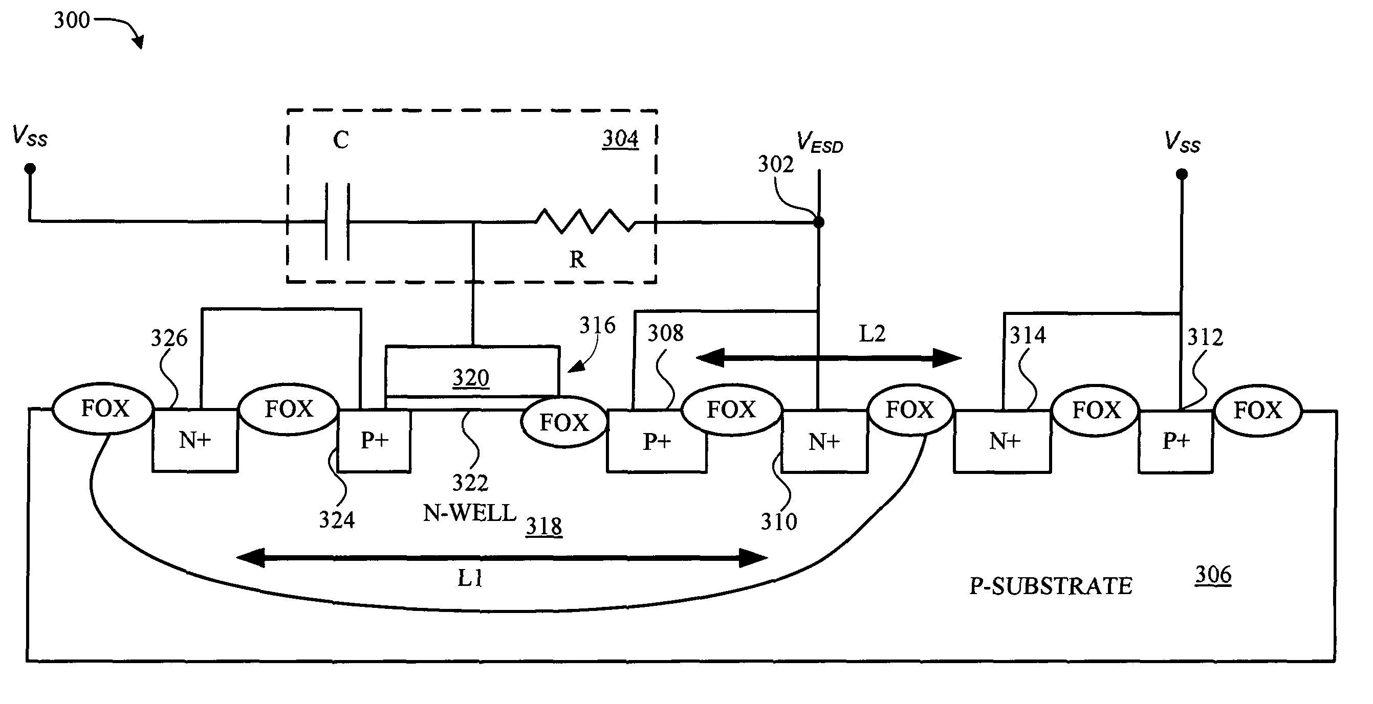
[0017]The present invention is directed generally to a fast triggered SCR (silicon controlled rectifier) that can trigger at a low enough voltage to protect thin oxides in integrated circuits from various electrical transients, including electrostatic discharge (ESD).

[0018]In the following description, for purposes of explanation, numerous specific details are set forth in order to provide a thorough understanding of the present invention. It will be evident, however, to one skilled in the art that the present invention may be practiced without these specific details. In other instances, well-known structures, and techniques are not shown in detail or are shown in block diagram form in order to avoid unnecessarily obscuring an understanding of this description.

[0019]Reference in the description to “one embodiment” or “an embodiment” means that a particular feature, structure, or characteristic described in connection with the embodiment is included in at least one embodiment of the ...


PUM


Abstract

A protection circuit and method are provided for protecting semiconductor devices from electrostatic discharge (ESD). Generally, the ESD protection circuit includes a silicon controlled rectifier (SCR) formed in a substrate and configured to transfer charge from a protected node to a negative power supply, VSS, during an ESD event, and a trigger device to activate transfer of charge by the SCR when a voltage on the protected node reaches a predetermined trigger voltage. The trigger device includes a gated-diode and MOS capacitor formed in a well formed in the substrate, the trigger device configured to inject electrons into the well during charging of the MOS capacitor, forward biasing a node of the SCR, hence allowing fast triggering of the SCR device. The trigger voltage can be set independent of a holding voltage by adjusting the length of the well and area of the capacitor. Other embodiments are also disclosed.

Description

CROSS-REFERENCE TO RELATED APPLICATIONS[0001]The present application claims the benefit of priority under 35 U.S.C. 119(e) to U.S. Provisional Patent Application Ser. No. 60 / 761,528 filed Jan. 24, 2006, entitled A Fast Capacitor Triggered SCR ESD Clamp for CMOS; which application is hereby incorporated by reference.TECHNICAL FIELD[0002]This invention relates to semiconductor devices and, more particularly, to protection devices for protecting integrated circuits from various electrical transients, including electrostatic discharge.BACKGROUND OF THE INVENTION[0003]As integrated circuit (IC) geometries continue to shrink, susceptibility to electrostatic discharge (ESD) damage increases. In particular, decreasing gate oxide thicknesses in MOS (metal-oxide-semiconductor) devices relative to breakdown voltage has resulted in an increased susceptibility to damage from the application of excessive voltages. During an ESD event, charge is transferred between one or more pins of the integrat...

Claims


Application Information

Patent Timeline
IPC IPC(8): H01L23/62
CPCH01L27/0262
Inventor WALKER, ANDREWPUCHNER, HELMUT
Owner CYPRESS SEMICON CORP
Learn More