
Triodes using nanofabric articles and methods of making the same

a technology of nanofabric articles and nanoelectronic devices, which is applied in the manufacture of electrode systems, electric discharge tubes/lamps, and tubes with electrostatic controls, etc. it can solve the problems of shortening the service life of vacuum tubes, requiring large thermal powers for electron emission, and reducing the size of the effect of performance improvemen

Inactive Publication Date: 2012-02-14
NANTERO
View PDF98 Cites 5 Cited by
  • Summary
  • Abstract
  • Description
  • Claims
  • Application Information

AI Technical Summary

Benefits of technology

The present invention describes a new type of vacuum tube that can be used in vacuum field emission devices. These devices can be smaller, lighter, and more easily integrated into CMOS circuits than current devices. The new vacuum tubes can have improved performance, reduced size, and can be fabricated using carbon nanotube films. The invention also provides devices with multiple vacuum tubes and methods of making them. The technical effects of the invention include improved performance, reduced size, and simplified fabrication processes.

Problems solved by technology

But the limits of these tubes were soon reached.
Because of problems inherent in these tube devices, modem integrated circuits have surpassed and replaced vacuum tube technology for fabrication of computer and electronic systems.
The problems include: leakage, the metal that emitted electrons in the vacuum tubes burned out, the requirement of large thermal powers for electron emission and large circuits took too much energy to run, etc.
Early computers were built with over 10,000 vacuum tubes and occupied huge amounts of space.
However, even with current high-speed semiconductor technology, power amplification is still a problem for the gigahertz frequencies.
Such disadvantages associated with solid-state semiconductor technology make vacuum tube technology appealing, since vacuum tubes have large electron speeds with much smaller power requirements.
To date, the fabrication of a triode (amplifier) using relatively low, useful voltages has not been feasible in integrated circuitry.
The large feature sizes employed by others to fabricate the micro-machined vacuum tubes has limited them to 3-terminals.
Fabricating higher order vacuum tubes such as tetrodes and pentodes is also not feasible with their designs and processes.

Method used


Image

  • Triodes using nanofabric articles and methods of making the same
  • Triodes using nanofabric articles and methods of making the same
  • Triodes using nanofabric articles and methods of making the same

Examples


Embodiment Construction

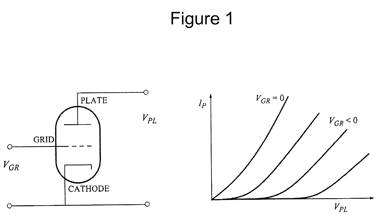
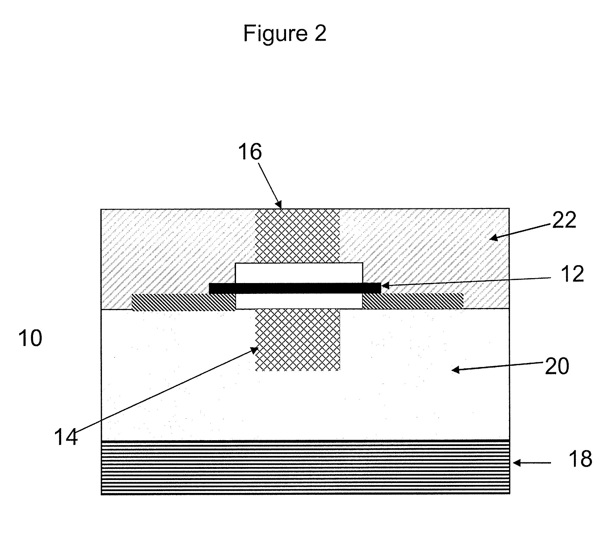
[0075]The present application generally relates to the utilization of carbon nanotube films, layers and fabrics in triodes and other related vacuum microelectronic and nanoelectronic devices and methods of making the same. More specifically, the present application relates to vacuum microelectronic and nanoelectronic devices and methods of manufacturing same using standard semiconductor processing techniques. The present application describes carbon nanotube-based vacuum tube devices, specifically triodes, but also higher-order vacuum tube devices including tetrodes and pentodes. In various embodiments, nanoscale triodes which use voltages of about an order of magnitude smaller, or even less than those voltages needed by the microtriodes of the current art are provided.

[0076]The many limitations of earlier triode designs point to the desirability of a CMOS compatible nanoscale vacuum-type structure that leverages the many advantages of carbon nanotube technology. CMOS compatible nan...


PUM

PropertyMeasurementUnit
sizesaaaaaaaaaa
thickaaaaaaaaaa
widthaaaaaaaaaa

Abstract

Vacuum microelectronic devices with carbon nanotube films, layers, ribbons and fabrics are provided. The present invention discloses microelectronic vacuum devices including triode structures that include three-terminals (an emitter, a grid and an anode), and also higher-order devices such as tetrodes and pentodes, all of which use carbon nanotubes to form various components of the devices. In certain embodiments, patterned portions of nanotube fabric may be used as grid / gate components, conductive traces, etc. Nanotube fabrics may be suspended or conformally disposed. In certain embodiments, methods for stiffening a nanotube fabric layer are used. Various methods for applying, selectively removing (e.g. etching), suspending, and stiffening vertically- and horizontally-disposed nanotube fabrics are disclosed, as are CMOS-compatible fabrication methods. In certain embodiments, nanotube fabric triodes provide high-speed, small-scale, low-power devices that can be employed in radiation-intensive applications.

Description

CROSS-REFERENCE TO RELATED APPLICATIONS[0001]This application claims priority under 35 U.S.C. §119(e) to U.S. Provisional Patent Application No. 60 / 931,227, entitled “Triodes Using Nanofabric Articles and Methods of Making the Same,” filed May 22, 2007.[0002]This application is related to the following applications which are assigned to the assignee of this application, and are hereby incorporated by reference in their entirety:[0003]U.S. Pat. No. 6,919,592, entitled Electromechanical Memory Array Using Nanotube Ribbons and Method for Making Same, filed on Jul. 25, 2001 [NAN1];[0004]U.S. Pat. No. 6,911,682, entitled Electromechanical Three-Trace Junction Devices, filed on Dec. 28, 2001 [NAN4];[0005]U.S. Pat. No. 6,706,402, entitled Nanotube Films and Articles, filed Apr. 23, 2002 [NAN6];[0006]U.S. patent application Ser. No. 10 / 341,005, entitled Methods of Making Carbon Nanotube Films, Layers, Fabrics, Ribbons, Elements and Articles, filed on Jan. 13, 2003 [NAN15]; and[0007]U.S. Pat...

Claims


Application Information

Patent Timeline
Patent Type & Authority Patents(United States)
IPC IPC(8): H01L29/02
CPCH01J3/021H01J19/38H01J21/10Y10S977/742H01J2203/0232
Inventor SEGAL, BRENT M.WARD, JONATHAN W.RUECKES, THOMAS
Owner NANTERO
Learn More