
Semiconductor light-emitting device and method of manufacturing the same

a technology of semiconductors and light-emitting devices, which is applied in the direction of vacuum evaporation coating, polycrystalline material growth, crystal growth process, etc., to achieve excellent mass productivity, low price, and sufficient light-emitting output

Inactive Publication Date: 2011-06-21
CITIZEN WATCH MFG +1
View PDF11 Cites 8 Cited by
  • Summary
  • Abstract
  • Description
  • Claims
  • Application Information

AI Technical Summary

Benefits of technology

"The invention aims to solve the problem of forming a thin film with good crystallinity on a heterogeneous substrate by using a ZnO buffer layer and a p-type layer in semiconductor light-emitting devices. The invention proposes a method for securely forming a high-quality p-type layer of ZnO directly on an n-type ZnO bulk single crystal substrate, which is excellent in mass productivity, light emission output, and environmental properties."

Problems solved by technology

However, ZnO is susceptible to have a defect of an oxygen vacancy and interstitial Zn atom, and has been regarded as difficult to form a p-type conductive layer, but many studies are under way to make ZnO p-type using nitrogen (N) as an acceptor impurity and fabricate a light emitting-device with a high efficiency using ZnO semiconductor.

Method used


Image

  • Semiconductor light-emitting device and method of manufacturing the same
  • Semiconductor light-emitting device and method of manufacturing the same
  • Semiconductor light-emitting device and method of manufacturing the same

Examples


embodiments

[0058]FIG. 5 shows a crystal growth system (hereinafter, referred to as a “reactive evaporation system”) using a reactive evaporation method assisted by plasma as an example of a ZnO thin film growth system using a method of manufacturing the semiconductor light-emitting device according to the invention.

[0059]The reactive evaporation system includes a bell jar 20 that is a reduced-pressure chamber, a not-shown gas supply apparatus for introducing oxygen and nitrogen thereinto, and a vacuum pump for bringing the inside of the bell jar 20 into a vacuum state. Penetrating through the wall surface of the bell jar 20, a gas supply port 21 for introducing oxygen and nitrogen and an exhaust port 22 for exhausting gas by the vacuum pump are provided.

[0060]In the bell jar 20, a dedicated substrate mask 23 for holding the n-type ZnO bulk single crystal substrate being a base of thin film growth is supported by an almost horizontal support member 24 in a mesh form. A heater 25 for heating the...


PUM

PropertyMeasurementUnit
resistivityaaaaaaaaaa
exciton binding energyaaaaaaaaaa
bandgap energyaaaaaaaaaa

Abstract

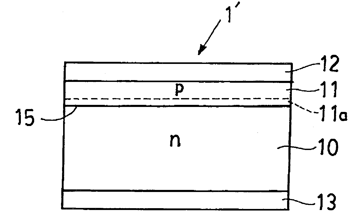
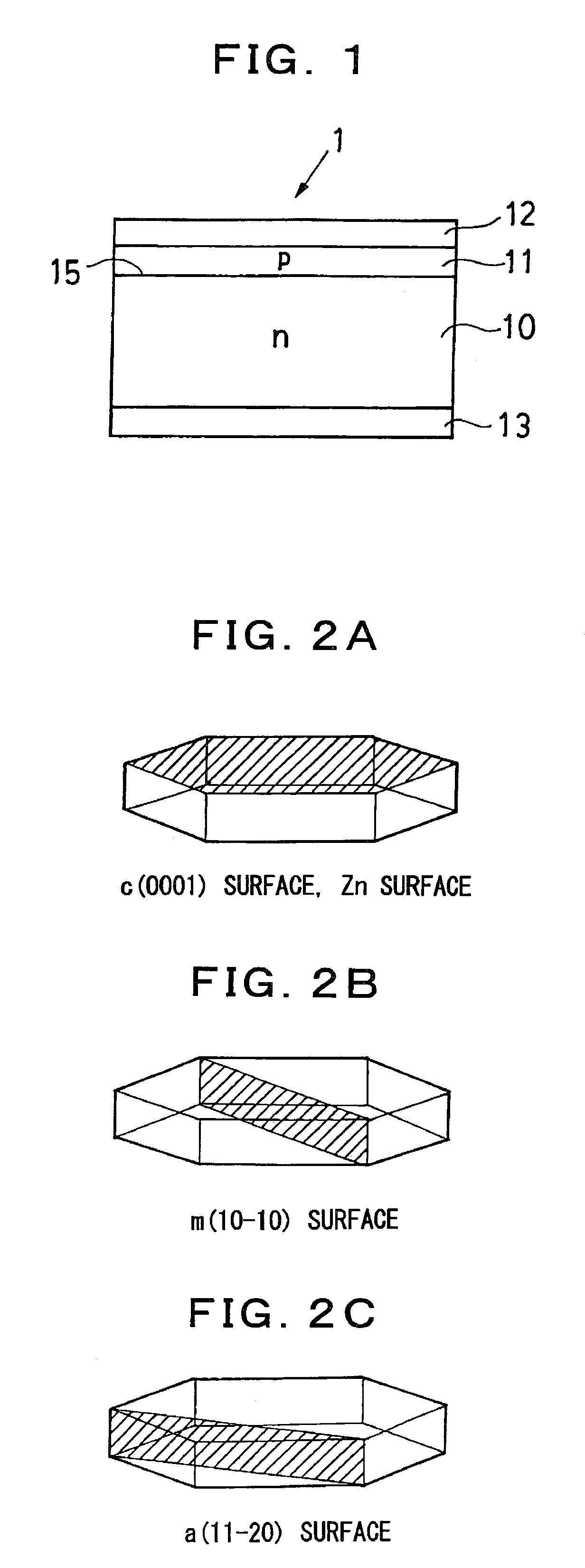
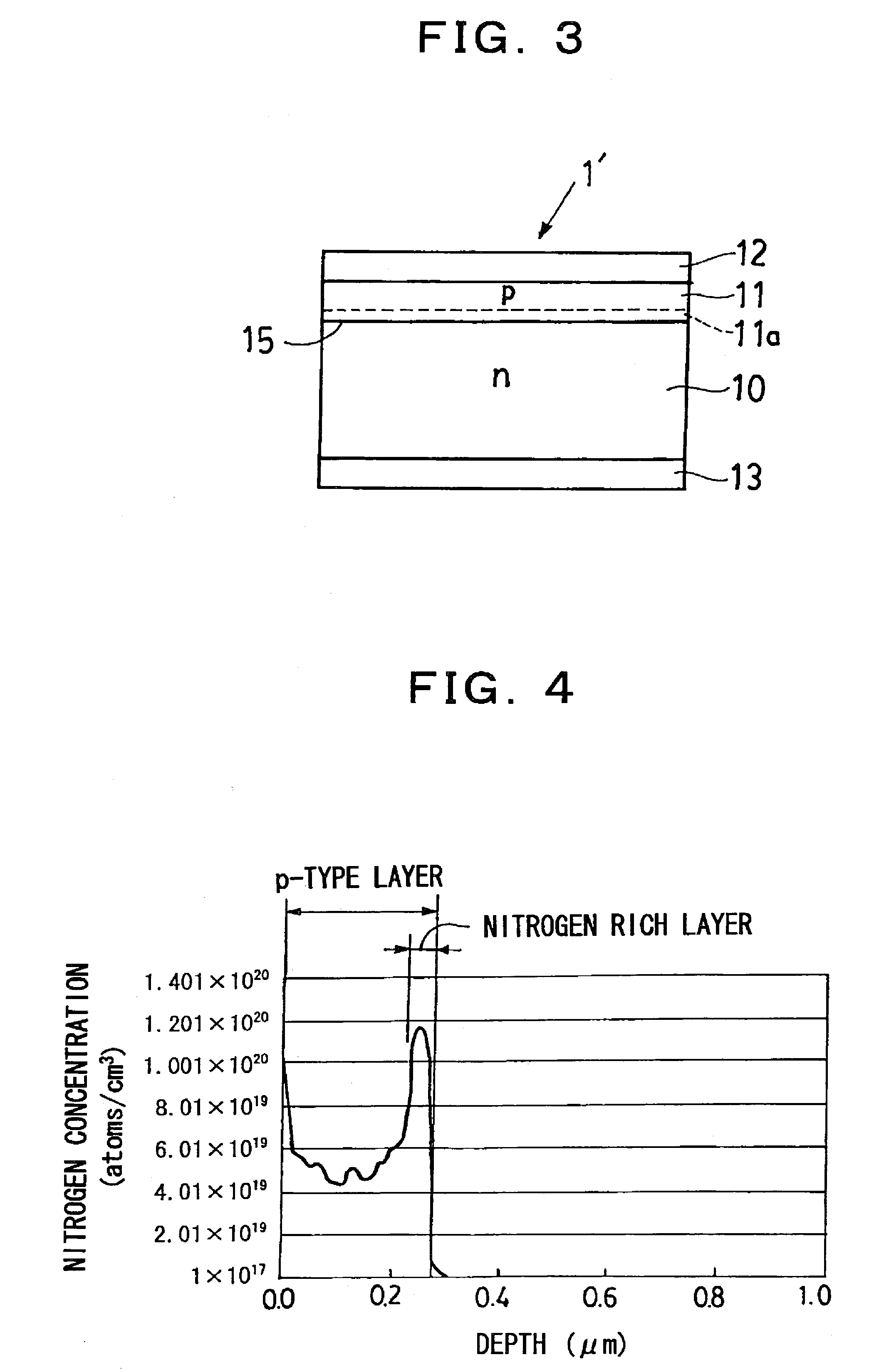
Disclosed is a semiconductor light-emitting device wherein a pn junction is formed by forming, as a p-type layer (11), a semiconductor thin film which is composed of a ZnO compound doped with nitrogen on an n-type ZnO bulk single crystal substrate (10) whose resistance is lowered by being doped with donor impurities. It is preferable to form the p-type layer (11) on a zinc atom containing surface of the n-type ZnO bulk single crystal substrate (10).

Description

TECHNICAL FIELD[0001]The present invention relates to a semiconductor light-emitting device suitable for emission of ultraviolet light, blue light, or white light, and a method of manufacturing the same.BACKGROUND TECHNOLOGY[0002]Zinc oxide (ZnO) is a direct transition semiconductor having a bandgap energy of about 3.4 eV and having a quite high exciton binding energy of 60 meV, and thus can realize a light-emitting device with a high efficiency and low power consumption. In addition, zinc oxide has characteristics such as a low raw material price and harmless to environment and human body and thus can provide a light-emitting device which is low in price and excellent in environmental properties.[0003]However, ZnO is susceptible to have a defect of an oxygen vacancy and interstitial Zn atom, and has been regarded as difficult to form a p-type conductive layer, but many studies are under way to make ZnO p-type using nitrogen (N) as an acceptor impurity and fabricate a light emitting...

Claims


Application Information

Patent Timeline
Patent Type & Authority Patents(United States)
IPC IPC(8): H01L29/10H01L33/12H01L33/16H01L33/28
CPCC23C14/042C23C14/086C23C14/32C30B23/00C30B23/02H01L33/285H01L21/02403H01L21/02433H01L21/02554H01L21/02576H01L21/02609C30B29/16
Inventor NAKAGAWA, AKIRAKASHIWABA, YASUBENIIKURA, IKUO
Owner CITIZEN WATCH MFG
Learn More