Light emitting device
a light-emitting device and light-emitting technology, which is applied in the manufacture of semiconductor/solid-state devices, semiconductor devices, electrical devices, etc., can solve the problems of large chip mounts, difficult to mount chips with large size, and large light-emitting mounts, etc., and achieve high light-emitting efficiency and thin body
- Summary
- Abstract
- Description
- Claims
- Application Information
AI Technical Summary
Benefits of technology
Problems solved by technology
Method used
Image
Examples
first embodiment
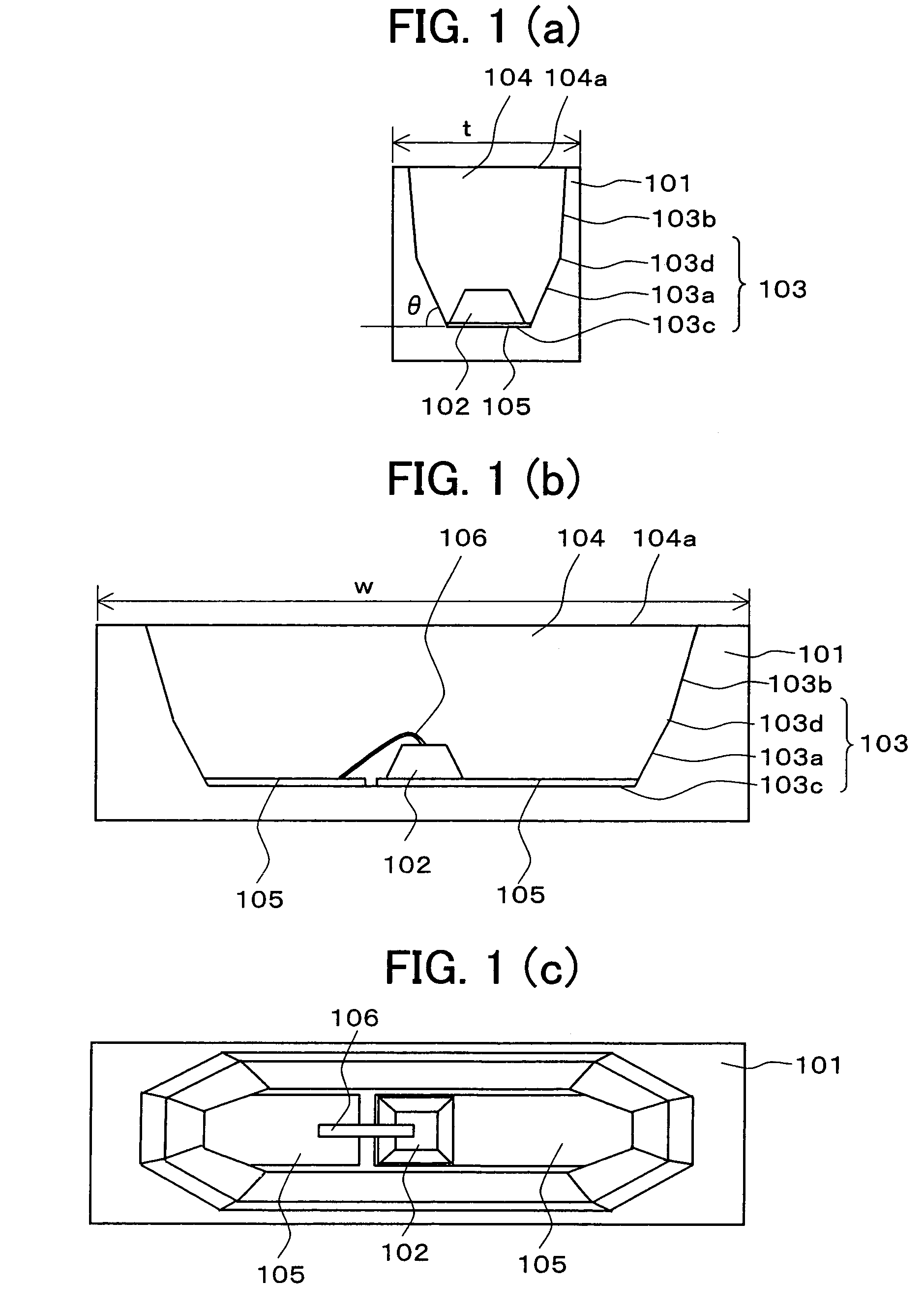
[0049]Referring to FIGS. 1 through 4, the following describes an embodiment of a light emitting device according to the present invention.
[0050]FIG. 1(a) is a cross-sectional view of the light emitting device according to the present embodiment.
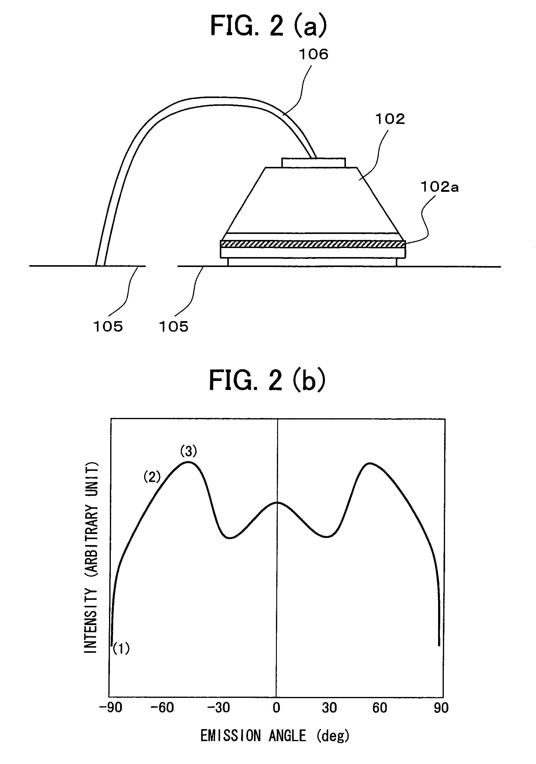
[0051]The light emitting device includes: a substantially rectangular package body (hereinafter referred to as package 101) having a dish-shaped concave portion; and an LED chip (hereinafter referred to as chip 102) shown in FIG. 2(a).
[0052]The concave portion constitutes a reflector 103 having a bottom surface 103c and a side wall provided with an angle along an outer edge of the bottom surface. In order to have a reflector function, the reflector 103 may utilize reflection characteristics of the package 101 itself in a case where the package 101 is constituted by a white package, or may separately process a side wall of the concave portion so as to improve reflectivity of the concave portion. For example, a reflective film may be formed on ...
second embodiment
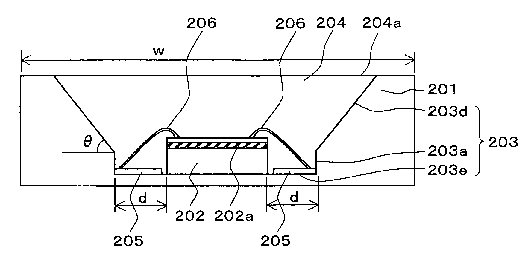
[0092]Referring to FIGS. 5 through 9, the following describes another embodiment of a light emitting device according to the present invention.
[0093]FIG. 5(a) is a cross sectional view of the light emitting device according to the present embodiment.
[0094]The light emitting device includes: a rectangular package body having a dish-shaped concave portion (hereinafter referred to as package 201); and a chip 202 having a light emitting section, i.e., an active layer, formed in the vicinity of a top surface of the chip 202 as shown in FIG. 5(a) (hereinafter referred to as junction up chip).
[0095]The concave portion constitutes a reflector 203 having a depressed region and an inclined plane provided along an edge of the depressed region.
[0096]The depressed region has a bottom surface 203e and a vertical plane 203a provided along an outer edge of the 203e so as to be substantially vertical to the bottom surface 203e.
[0097]The depressed region has a depth being substantially equivalent to...
PUM
 Abstract
Description
Claims
Application Information
 - R&D
- Intellectual Property
- Life Sciences
- Materials
- Tech Scout
- Unparalleled Data Quality
- Higher Quality Content
- 60% Fewer Hallucinations
Browse by: Latest US Patents, China's latest patents, Technical Efficacy Thesaurus, Application Domain, Technology Topic, Popular Technical Reports.
© 2025 PatSnap. All rights reserved.Legal|Privacy policy|Modern Slavery Act Transparency Statement|Sitemap|About US| Contact US: help@patsnap.com


