Eureka AIR delivers breakthrough ideas for toughest innovation challenges, trusted by R&D personnel around the world.

Semiconductor device having multiport memory

a technology of semiconductor devices and memory, applied in semiconductor devices, digital storage, instruments, etc., can solve the problems of difficult to sufficiently predict the degree of mutual interference, possible delay in the rise time (or fall time) of waveforms, and similar problems accompanying asynchronous operations. , to achieve the effect of reducing interference, expanding noise margin, and increasing circuit area

Active Publication Date: 2011-05-10
RENESAS ELECTRONICS CORP
View PDF9 Cites 22 Cited by
  • Summary
  • Abstract
  • Description
  • Claims
  • Application Information

AI Technical Summary

Benefits of technology

[0012]With this, it is possible to reduce interference between different ports, and to achieve an expanded noise margin. Also, as compared with an exemplary case of alternate disposition of a first word line and a second word line, the expansion of the noise margin can be intended with a small area. In addition, further expansion of the noise margin can be obtained by inserting a shield line between the first word line and the second word line. In this case, the problem of an area increase does not occur because no shield line is necessary between the word lines of an identical port (between neighboring first word lines and between neighboring second word lines).
[0015]With this, in the intersection portion between the first wiring line and the second wiring line, it becomes possible to reduce interference between the first wiring line and the second wiring line, that is, interference between different ports, possibly caused by mutual approximation, enabling an expanded noise margin. Additionally, such the intersection of wiring lines as described above does not occur when such the configuration is used that the first selector circuit is disposed on one side of a rectangular area, having a plurality of memory cells disposed therein, and the second selector circuit is disposed on the opposite side thereto. However, in the above configuration, there is produced a side effect of an increased circuit area, as compared with the configuration having both the first selector circuit and the second selector circuit disposed on one side, as described earlier.
[0016]Further, the semiconductor device according to one embodiment of the present invention includes a shield line between a first control signal for controlling the above-mentioned first selector circuit and a second control signal for controlling the second selector circuit. Specifically, the first control signal, the second control signal and the shield line extend in a direction that the first selector circuit and the second selector circuit are disposed in order (that is, an extension direction of the word lines), and further, the first control signal is disposed in juxtaposition on one side across the shield line and the second control signal is disposed in juxtaposition on the other side. With this, the interference between the first control signal and the second control signal, namely, the interference between different ports can be reduced, and the expansion of the noise margin can be attained.
[0017]Using the semiconductor device according to one embodiment of the present invention, it is possible to reduce the interference between different ports, to expand the noise margin, and to obtain the noise margin expansion with a small area.

Problems solved by technology

However, from a different point of view, the exemplary configuration shown in FIG. 20 is configured to have a word line WLA (or WLB) for port A (or port B) sandwiched by word lines WLB (or WLA) for port B (or port A), and therefore, there is a possible problem caused by interference between different ports. FIG. 21 shows an explanatory diagram illustrating one example of operation waveforms between different ports and in an identical port. FIG. 22 shows an explanatory diagram illustrating one example of a trouble due to interference between ports.
If the above situation occurs, as shown in FIG. 22 for example, when the activation timing of the word line for the first port and the deactivation timing of the word line for the second port coincides, a delay may possibly be produced in the rise time (or fall time) of the waveform because of mutually affecting interference.
Although the word line is taken as an example in the above description, the similar problem accompanying asynchronous operation may occur in regard to mutually neighboring bit lines for different ports, and in regard to other signal lines also.
On the other hand, in regard to signals for different ports, activation and deactivation are made mutually asynchronously and at arbitrary timing (in other words, there are infinite number of combinations in the phase relation between the first port signals and the second port signals in the example shown in FIG. 21), and therefore, it is difficult to sufficiently predict the degree of mutual interference.

Method used


Image

  • Semiconductor device having multiport memory
  • Semiconductor device having multiport memory
  • Semiconductor device having multiport memory

Examples


embodiment 1

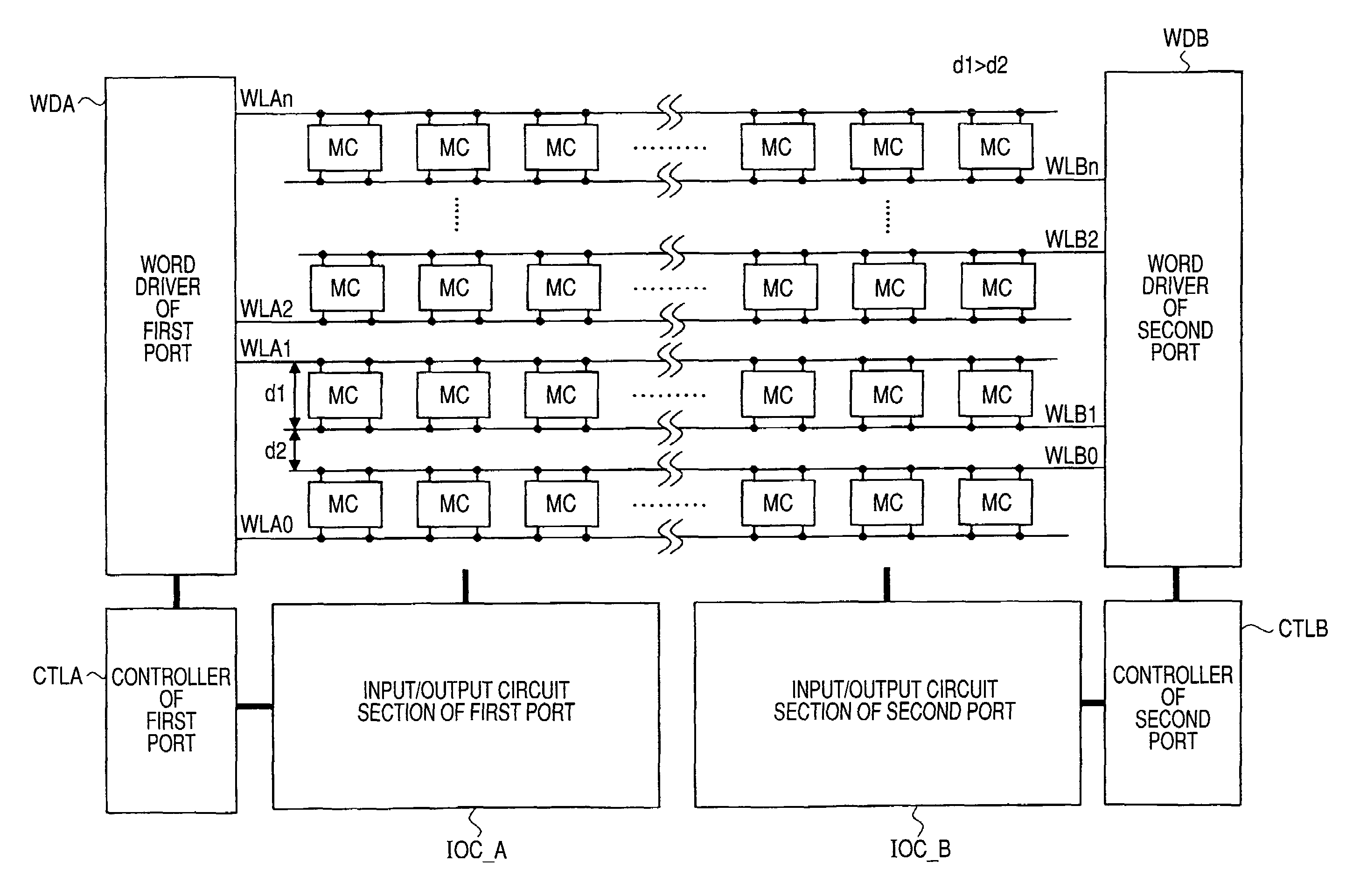
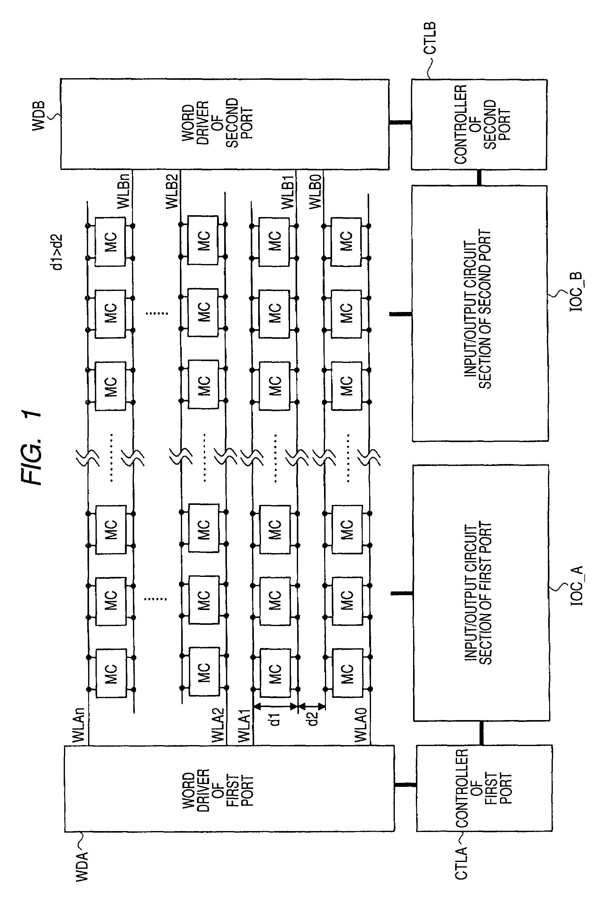
[0044]FIG. 1 shows a block diagram illustrating one exemplary configuration of a semiconductor device according to an embodiment 1 of the present invention. FIG. 2 shows a circuit diagram illustrating an exemplary configuration of a memory cell MC in the semiconductor device shown in FIG. 1. The semiconductor device shown in FIG. 1 includes a plurality of memory cells MC disposed in the row and column shape (matrix shape), a word driver WDA for a first port (port A), a controller CTLA and an input / output circuit section IOC_A, and further, a word driver WDB for a second port (port B), a controller CTLB and an input / output circuit section IOC_B.

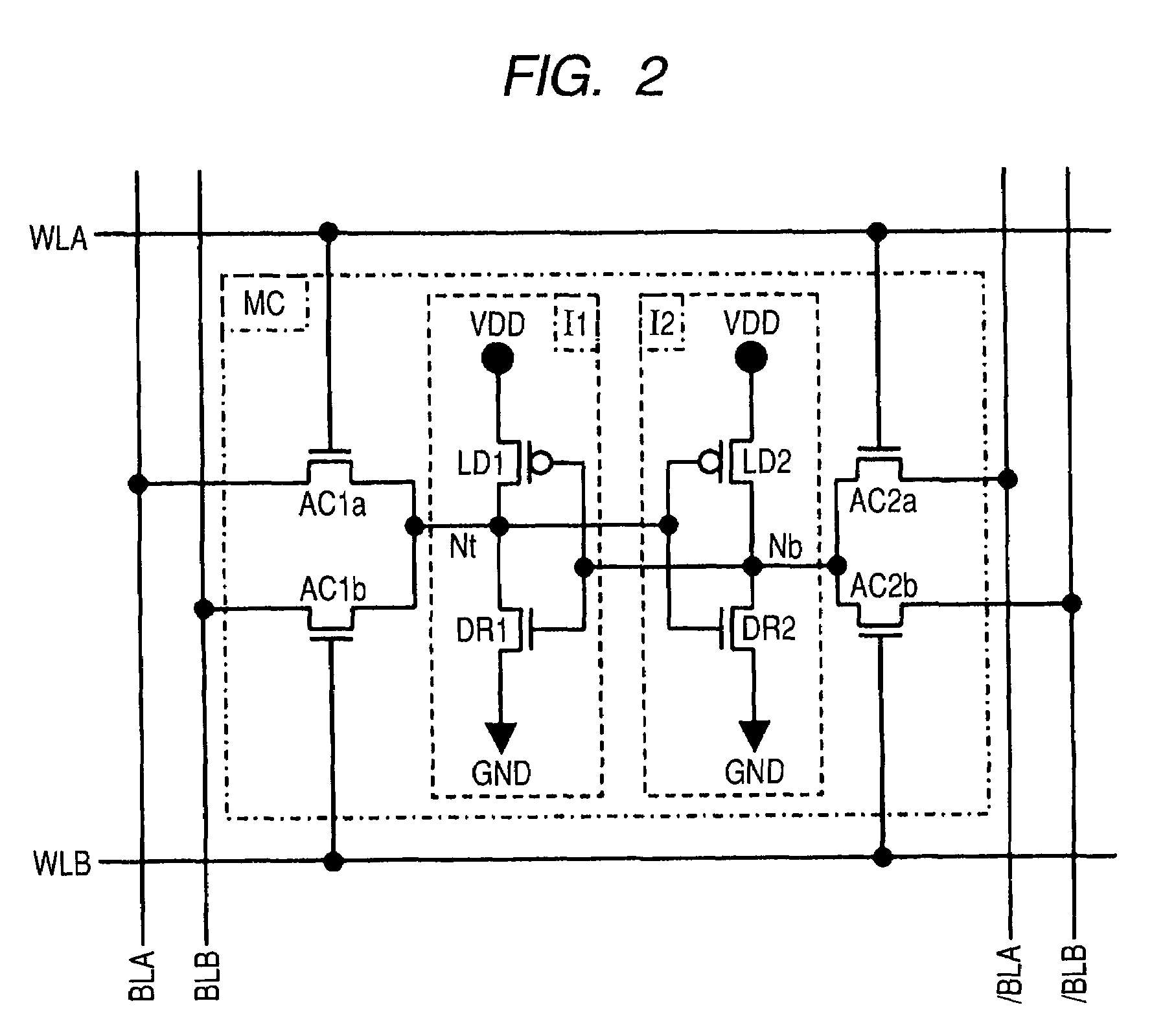
[0045]As shown in FIG. 2, each memory cell MC is a so-called SRAM memory cell, which includes two driver transistors DR1 and DR2, two load transistors LD1 and LD2, and four access transistors AC1a, AC1b, AC2a and AC2b. Here, the driver transistors DR1, DR2 and access transistors AC1a, AC1b, AC2a, AC2b are configured of NMOS transistors, while ...

embodiment 2

[0076]FIG. 7 shows a plan view illustrating an exemplary configuration of a semiconductor device deformed from the layout shown in FIG. 4, according to an embodiment 2 of the present invention. As shown in FIG. 7, the semiconductor device according to the present embodiment 2 has a principal feature of further providing a shield line SLD, which extends in juxtaposition with the word line between the word lines of different ports (between WLA and WLB), in addition to the word line layout similar to FIG. 4.

[0077]With the provision of such the shield line SLD, it becomes possible to further expand a noise margin between the word lines of different ports. Also, if the layout area of each memory cell can be restrained, it becomes possible to further decrease the pitch d1 between WLA and WLB as compared with the pitch d1 in case of FIG. 4 due to a shield effect, and thus, it becomes possible to expand the noise margin with a smaller area than the case of embodiment 1.

[0078]Also, since the...

embodiment 3

[0087]FIG. 14 shows a block diagram illustrating one exemplary configuration of a semiconductor device according to an embodiment 3 of the present invention. As compared with the semiconductor device shown in FIG. 1, the principal features of the semiconductor device shown in FIG. 14 lie in: (1) the disposition of input / output circuit sections IOC_A, IOC_B; (2) the wiring layout from the bit line to the IOC_A, IOC_B; and (3) the disposition of each control line when the controllers CTLA, CTLB control the IOC_A, IOC_B. In the following, descriptions on the portions overlapped with FIG. 1 are omitted.

[0088]In FIG. 14, the controller CTLA of a first port (port A) includes a latch section ADD_LT for latching an address signal for the first port being input externally, a decoder DEC for decoding the above address signal, and a Y selection buffer section YSEL_BF for outputting a Y selection signal etc. corresponding to a Y address for the first port. Similarly, the controller CTLB of a se...


PUM


Abstract

A semiconductor device enabling expansion of a noise margin. For example, in a memory area in which each memory cell MC is coupled to a word line WLA for a first port and a word line WLB for a second port, and a plurality of memory cells MC is disposed in a matrix shape, each word line is disposed in the order like WLA0, WLB0, WLB1, WLA1, WLA2, . . . . Further, a pitch d2 between WLA-WLA and between WLB-WLB is made smaller than a pitch d1 between WLA-WLB. As such, the word lines of an identical port are disposed at the pitch d2 on one of both sides of a certain word line as a criterion, while the word lines of different ports are disposed at the pitch d1 on the other. With the above configuration, for example, as compared with a case of alternately disposing WLA and WLB, interference between ports can be reduced even with a small area, and the noise margin can be expanded.

Description

CROSS-REFERENCE TO RELATED APPLICATION[0001]The present application claims priority from Japanese patent application No. 2007-226451 filed on Aug. 31, 2007, the content of which is hereby incorporated by reference into this application.BACKGROUND OF THE INVENTION[0002]The present invention relates to a semiconductor device, and more particularly to a technique which is useful when applied to a semiconductor device such as a multiport SRAM (Static Random Access Memory).[0003]As an example, in Japanese Unexamined Patent Publication No. 2004-335535 (hereafter referred to as Patent Document 1), there is described a multiport memory of SRAM configuration having a layout such that a word line corresponding to a first port and a word line corresponding to a second port are disposed alternately. According to the above configuration, noise can be reduced without increasing a memory cell area because it is possible to avoid such a situation that coupling noise is simultaneously induced to a w...

Claims


Application Information

Patent Timeline
Patent Type & Authority Patents(United States)
IPC IPC(8): G11C5/02
CPCG11C7/1075G11C8/16G11C11/412H01L27/1104G11C5/02H01L27/0207G11C11/413H01L27/11H10B10/00H10B10/12G11C11/41G11C5/06G11C11/417
Inventor FUNANE, KIYOTADASHIBATA, KENSHIMAZAKI, YASUHISA
Owner RENESAS ELECTRONICS CORP
Why Eureka
Eureka Blog
Learn More