Film bulk acoustic wave resonator and method for manufacturing the same
a technology of acoustic wave resonators and films, which is applied in piezoelectric/electrostrictive/magnetostrictive devices, piezoelectric/electrostriction/magnetostriction machines, electrical apparatuses, etc., can solve the problems of degrading the attenuation characteristics outside the pass band, and achieves high accuracy, easy production, and suppression of different resonance modes
- Summary
- Abstract
- Description
- Claims
- Application Information
AI Technical Summary
Benefits of technology
Problems solved by technology
Method used
Image
Examples
first embodiment
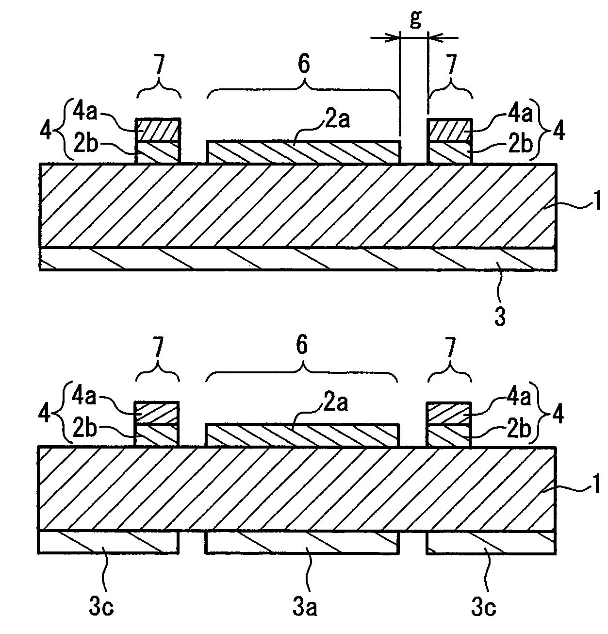
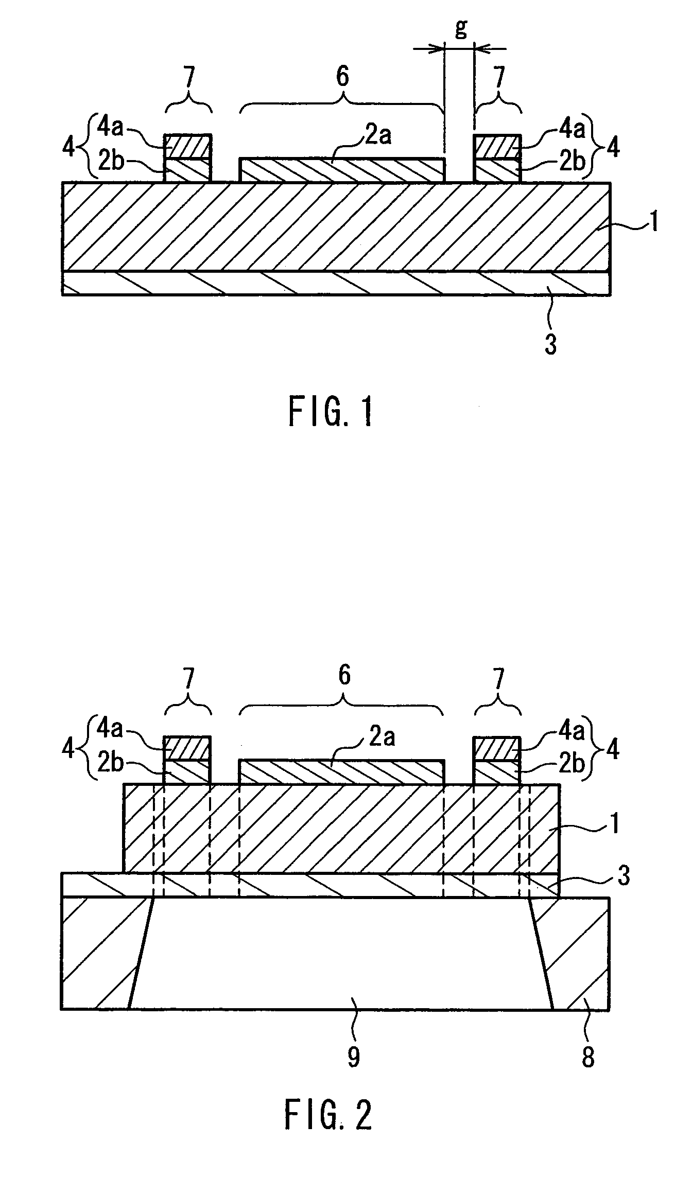
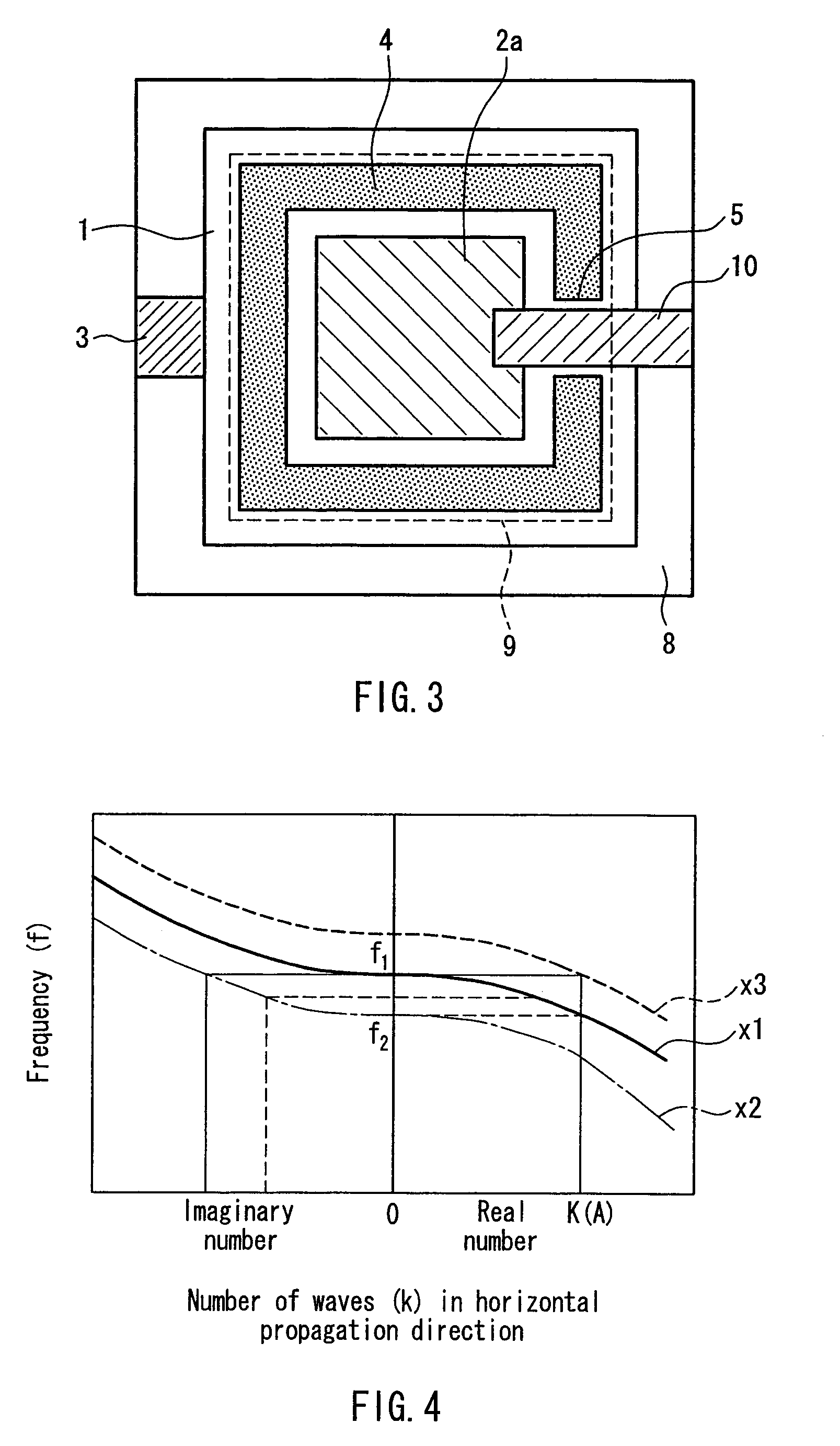
[0071]FIG. 1 is a cross sectional view showing an example of the structure of the resonance portion of the film bulk acoustic wave resonator according to a first embodiment of the present invention. FIG. 2 is a cross sectional view showing a film bulk acoustic wave resonator including a support structure for the resonance portion shown in FIG. 1. FIG. 3 is a top view showing an example of the structure in which wiring is included in the film bulk acoustic wave resonator of FIG. 2.
[0072]The film bulk acoustic wave resonator according to this embodiment has a resonance portion structure as shown in FIG. 1. Specifically, an upper electrode 2a is formed on a piezoelectric body 1, and a lower electrode 3 is formed under the piezoelectric body 1. A first mass load material portion 4 is formed so as to surround the upper electrode 2a on the piezoelectric body 1. The upper electrode 2a, the piezoelectric body 1 and the lower electrode 3 together form a center region 6. The first mass load m...
second embodiment
[0095]FIG. 6 is a cross sectional view showing an example of the structure of the resonance portion of a film bulk acoustic wave resonator according to a second embodiment of the present invention. The film bulk acoustic wave resonator according to this embodiment has a structure in which a lower electrode 3a, a piezoelectric body 1 and an upper electrode 2 are formed, in this order, on a substrate (not shown). The lower electrode 3a is formed only within a center region 6. A second mass load material portion 12 is formed outside of the lower electrode 3a between the substrate and the piezoelectric body 1. The lower electrode 3a, the piezoelectric body 1 and the upper electrode 2 together form the center region 6, and the second mass load material portion 12, the piezoelectric body 1 and the upper electrode 2 together form a mass load region 7. The outer periphery of the lower electrode 3a and the inner periphery of the second mass load material portion 12 are spaced apart from each...
third embodiment
[0108]FIG. 9 is a cross sectional view showing an example of the structure of the resonance portion of a film bulk acoustic wave resonator according to a third embodiment of the present invention. The film bulk acoustic wave resonator of this embodiment has a structure in which, in the film bulk acoustic wave resonator of the first embodiment shown in FIG. 1, the lower electrode 3 is divided at the boundary region between the center region 6 and the mass load region 7 so as to be patterned into a center lower electrode 3a and a second mass load material portion 3c.
[0109]In the structure of FIG. 1, strictly speaking, the electric field applied between the upper electrode 2a and the lower electrode 3 is not limited to the thickness direction. For this reason, when one of the upper electrode 2a and the lower electrode 3 is not divided, vibration in an oblique direction also may be generated, which contributes to the generation of different resonance modes.
[0110]In contrast, by providi...
PUM
 Abstract
Description
Claims
Application Information
 - R&D
- Intellectual Property
- Life Sciences
- Materials
- Tech Scout
- Unparalleled Data Quality
- Higher Quality Content
- 60% Fewer Hallucinations
Browse by: Latest US Patents, China's latest patents, Technical Efficacy Thesaurus, Application Domain, Technology Topic, Popular Technical Reports.
© 2025 PatSnap. All rights reserved.Legal|Privacy policy|Modern Slavery Act Transparency Statement|Sitemap|About US| Contact US: help@patsnap.com


