Optical phase modulator
a phase modulator and optical phase technology, applied in non-linear optics, instruments, optics, etc., can solve the problems of inability to apply control of chirp quantity, weak electrical field confinement, and weak radio frequency characteristic, so as to promote impedance matching, increase the characteristic impedance of the electrode, and increase the operation stability
- Summary
- Abstract
- Description
- Claims
- Application Information
AI Technical Summary
Benefits of technology
Problems solved by technology
Method used
Image
Examples
first example
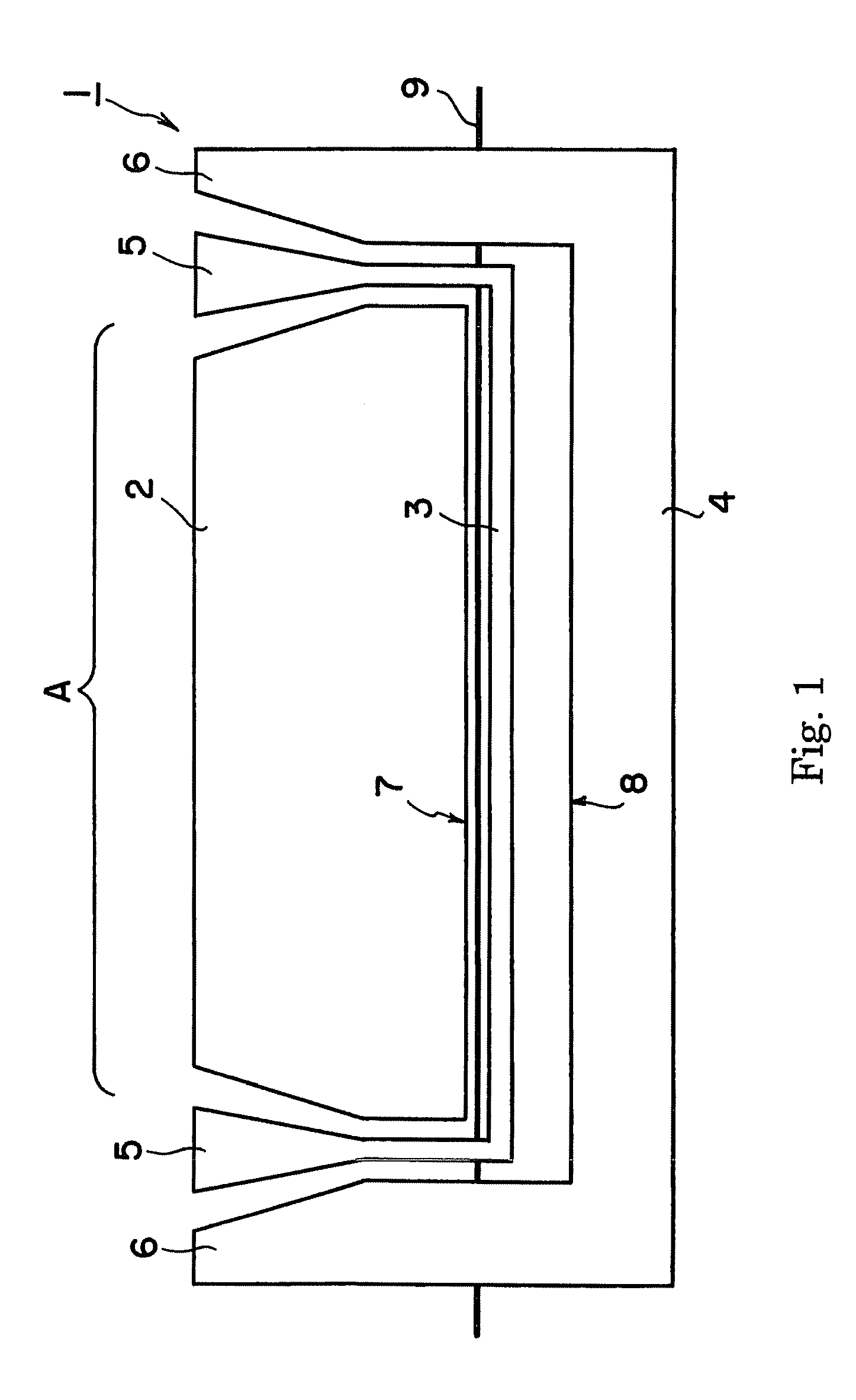
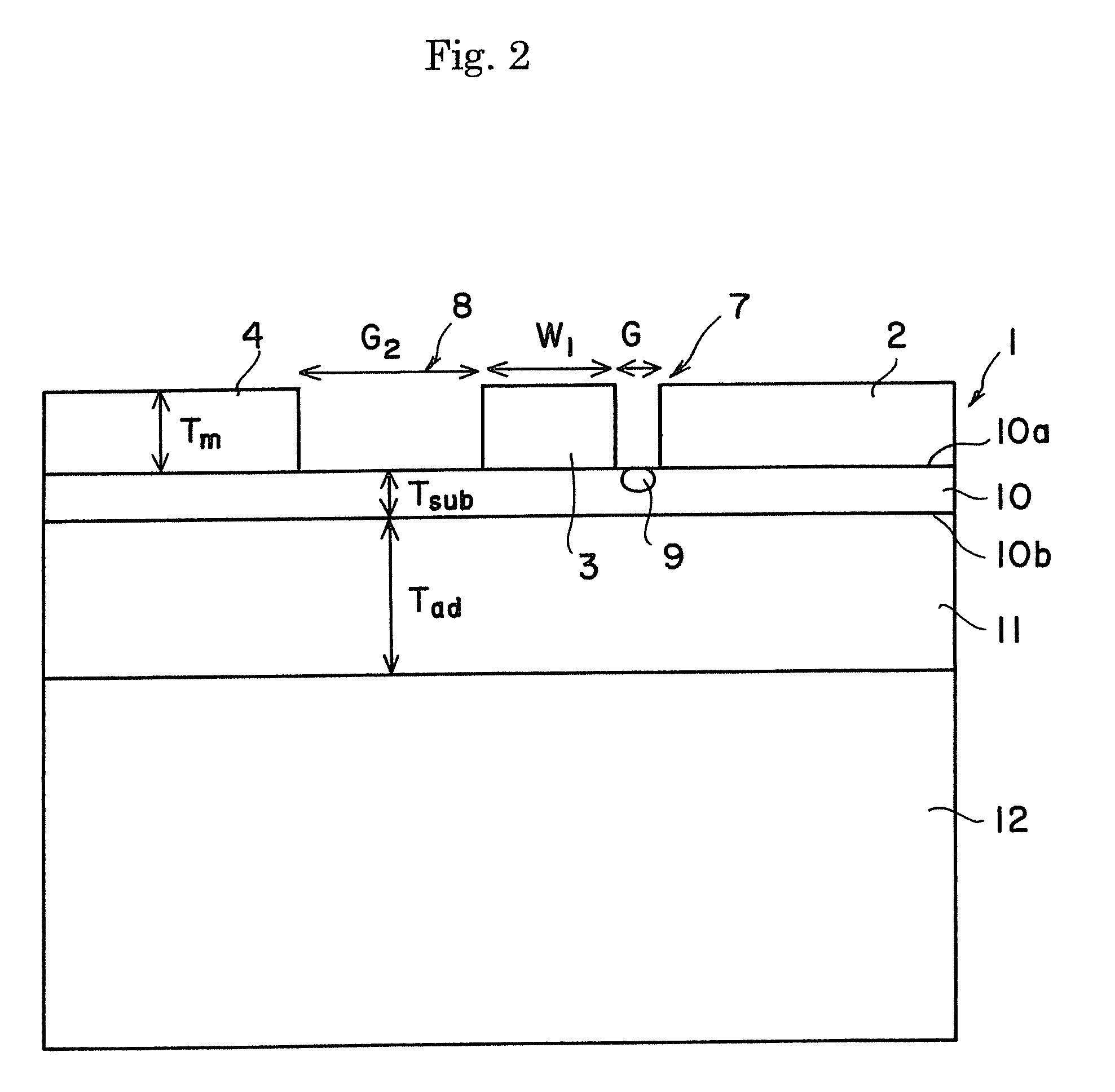
[0069]The optical phase modulator 1 as shown in FIGS. 1 and 2 was produced, and a phase modulation experiment was carried out. Sizes are set as follows (refer to FIG. 2).
[0070]G1=16 μm, G2=92 μm, W=38 μm, Tm=20 μm,
[0071]Tsub=7.0 μm, Tad=50 μm, and relative permittivity of the low dielectric constant layer 11: 4.0.
[0072]As the electric-optical substrate 10, an X-cut lithium niobate substrate was used. With this structure, the effective refractive index of microwave was 2.2, and the microwave and light are velocity-matched. The characteristic impedance was 43Ω. Moreover, the half-wave voltage Vπ decreased down to 3.3V when the interaction-length of the electrodes was 32 mm.
second example
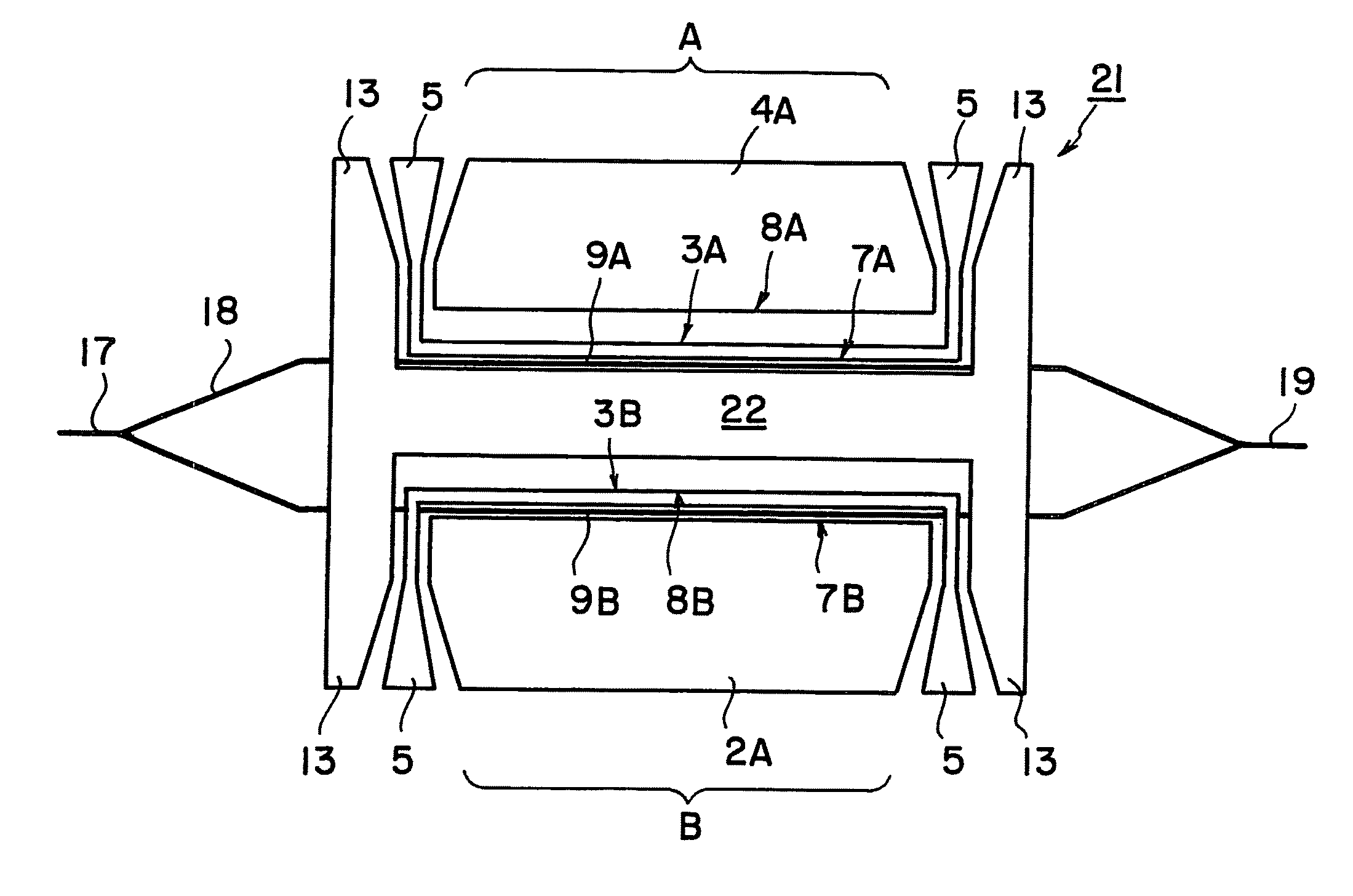
[0073]The optical phase modulator 21 as shown in FIGS. 3 and 4 was produced, and a phase modulation experiment was carried out. It should be noted that the following dimensions were set.
W=40 μm, G1=16.5 μm, G2=90 μm,
WGND=WGND2=WGND3=100 μm, Tsub=7 μm,
electrode thickness Tm=17 μm, and electrode interaction length L=3.2 cm.
[0074]As the electric-optical substrate 1, an X-cut lithium niobate substrate was used. With this structure, the effective refractive index of microwave was 2.2, and the microwave and light are velocity-matched. The following data were obtained under these conditions.
[0075]Electrode conductor loss α=0.33 dB·cm−1·GHz−1 / 2
[0076]Characteristic impedance Z=41 Ω
[0077]Half wave voltage Vπ=3.4 V
[0078]Product of half wave voltage and interaction length VπL=10.8 V·cm
[0079]3 dB band width ΔF3 dB=25 GHz
third example
[0080]Dependency on the ground electrode width WGND was investigated in the second example. In other words, in FIG. 4, only WGND was variously changed. As a result, when the ground electrode widths WGND were 50, 150, 200 and 500 μm, the electrode propagation loss α were respectively 0.34, 0.32 and 0.31 dB·cm−1·GHz−1 / 2. Even when WGND is decreased down to approximately 50 μm, it is appreciated that the electrode propagation loss does not change so much.
PUM
| Property | Measurement | Unit |
|---|---|---|
| thickness | aaaaa | aaaaa |
| width | aaaaa | aaaaa |
| thickness | aaaaa | aaaaa |
Abstract
Description
Claims
Application Information
 - R&D
- Intellectual Property
- Life Sciences
- Materials
- Tech Scout
- Unparalleled Data Quality
- Higher Quality Content
- 60% Fewer Hallucinations
Browse by: Latest US Patents, China's latest patents, Technical Efficacy Thesaurus, Application Domain, Technology Topic, Popular Technical Reports.
© 2025 PatSnap. All rights reserved.Legal|Privacy policy|Modern Slavery Act Transparency Statement|Sitemap|About US| Contact US: help@patsnap.com


